 Nick
Nick
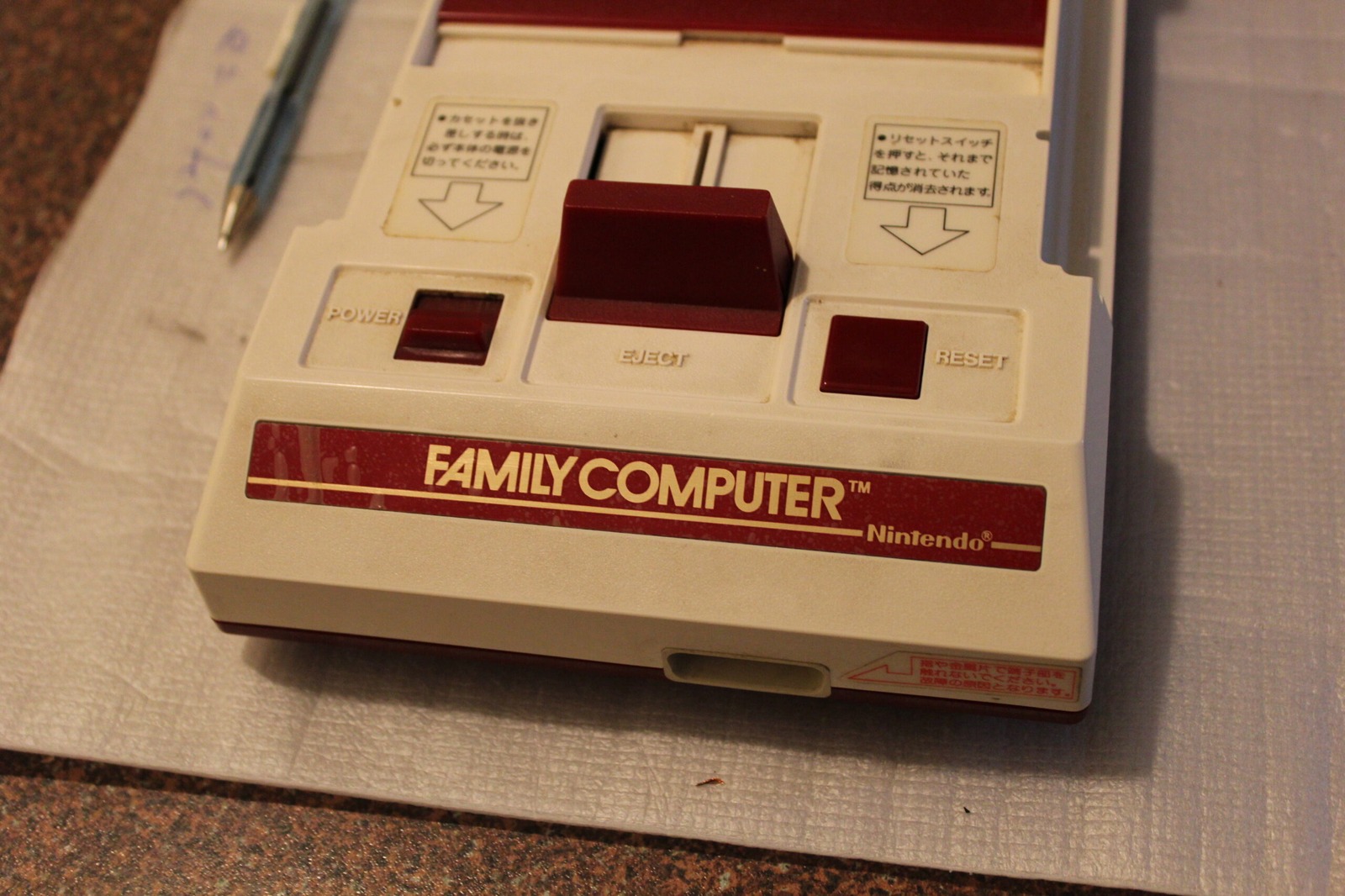
The Nintendo Family Computer. Ohhhh yeahhhh! Below are the first, second and third revisions of my attempt at an AV mod for the Famicom.
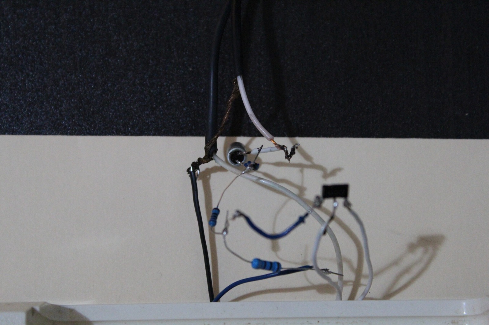
The first attempt was a proof of concept, hence the mess of cables. Functional yet hideous.
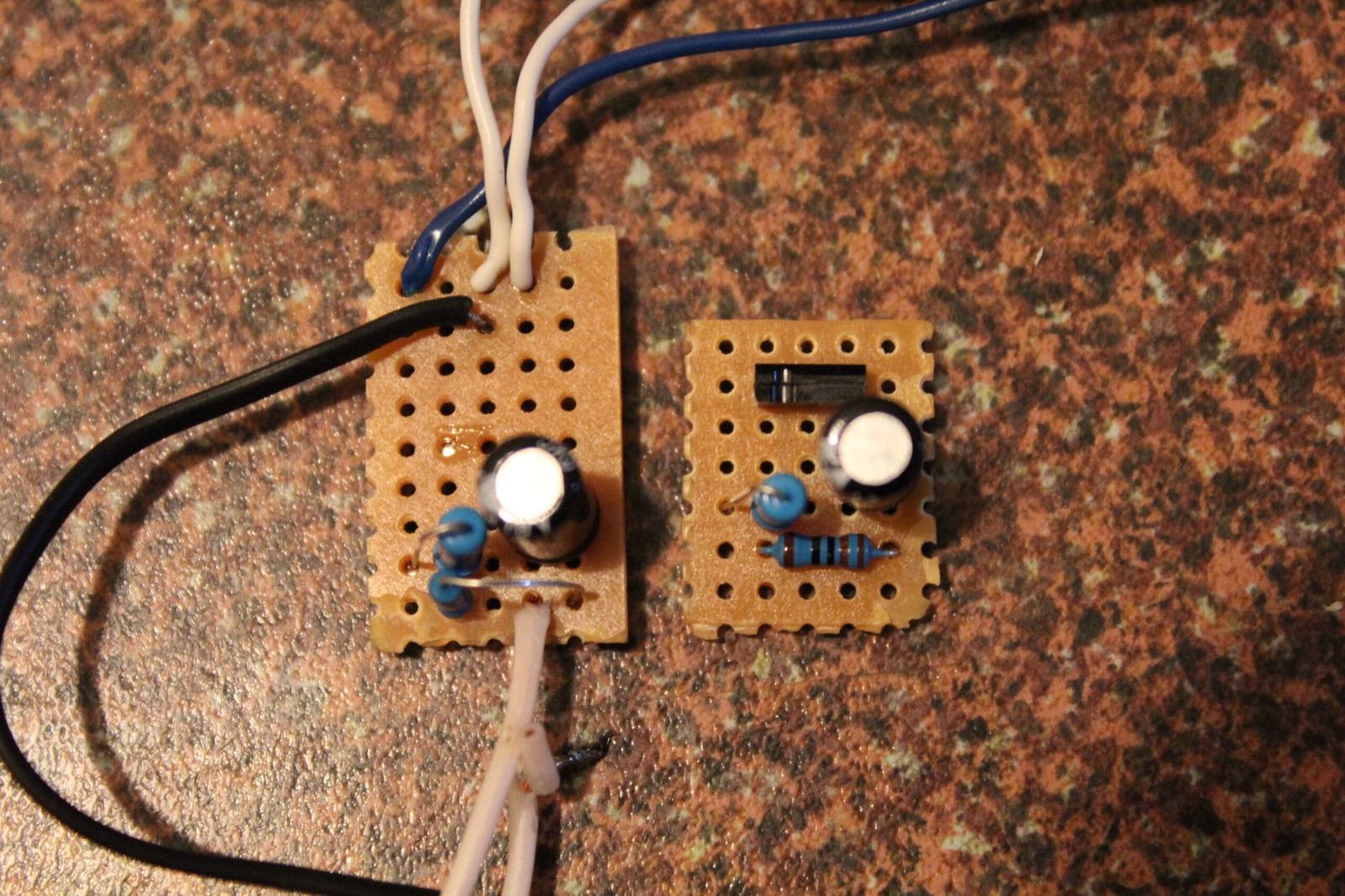
The second attempt used a slightly longer piece of prototyping board. I was building it with some fairly questionable parts, including a cable tie pressed into service as a wire for ground. It worked, but it was not what I wanted.
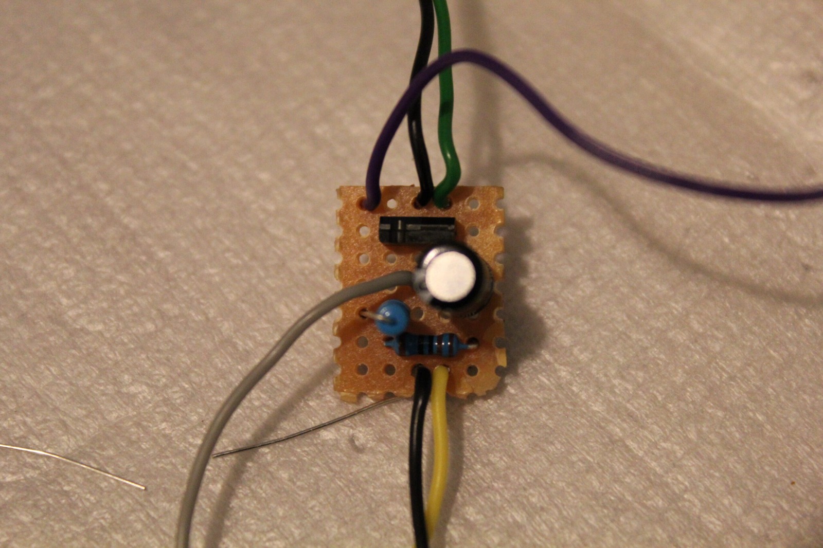
The final version was shrunk down to fit on a much smaller piece of prototyping board. A much better piece of hardware.
Parts used
This parts list documents the circuit that worked on this particular Famicom motherboard. Famicom board revisions differ, and later AV-mod designs use different component values and connection points, so treat this as a record of this build rather than a universal recipe.
- 1 x 110 ohm resistor, 0.25 W, 1% tolerance
- 1 x 300 ohm resistor, 0.5 W, 5% tolerance
- 2 x 220 uF, 16 V, 105°C electrolytic capacitors
- 1 x PNP transistor, reused from the Famicom mainboard in this build
- Flexible light-duty hookup wire or Kynar wire
- 7 x 5-hole prototyping board or stripboard
- 25 to 40 W soldering iron and solder
- RCA cables, plugs and sockets
To make it all come together and actually give us composite AV, read on!
Removing the video transistor
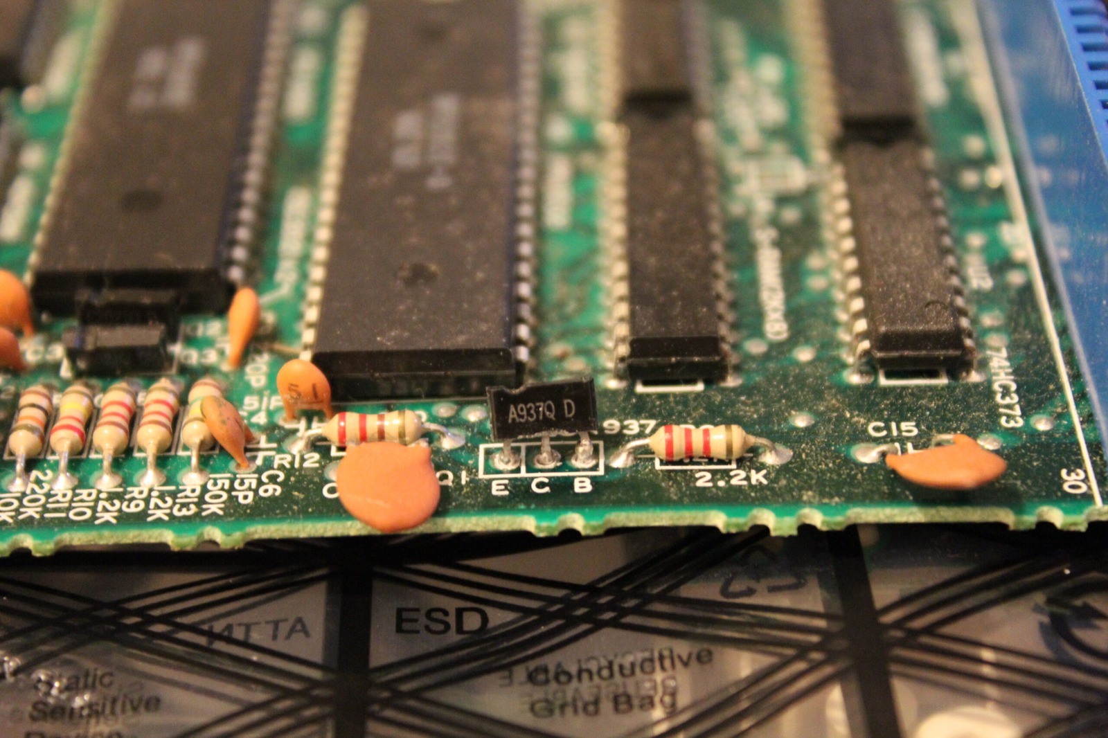 Half-desoldered A937Q D PNP transistor on the Famicom mainboard. Note the ECB on the mainboard. Emitter, Collector and Base.
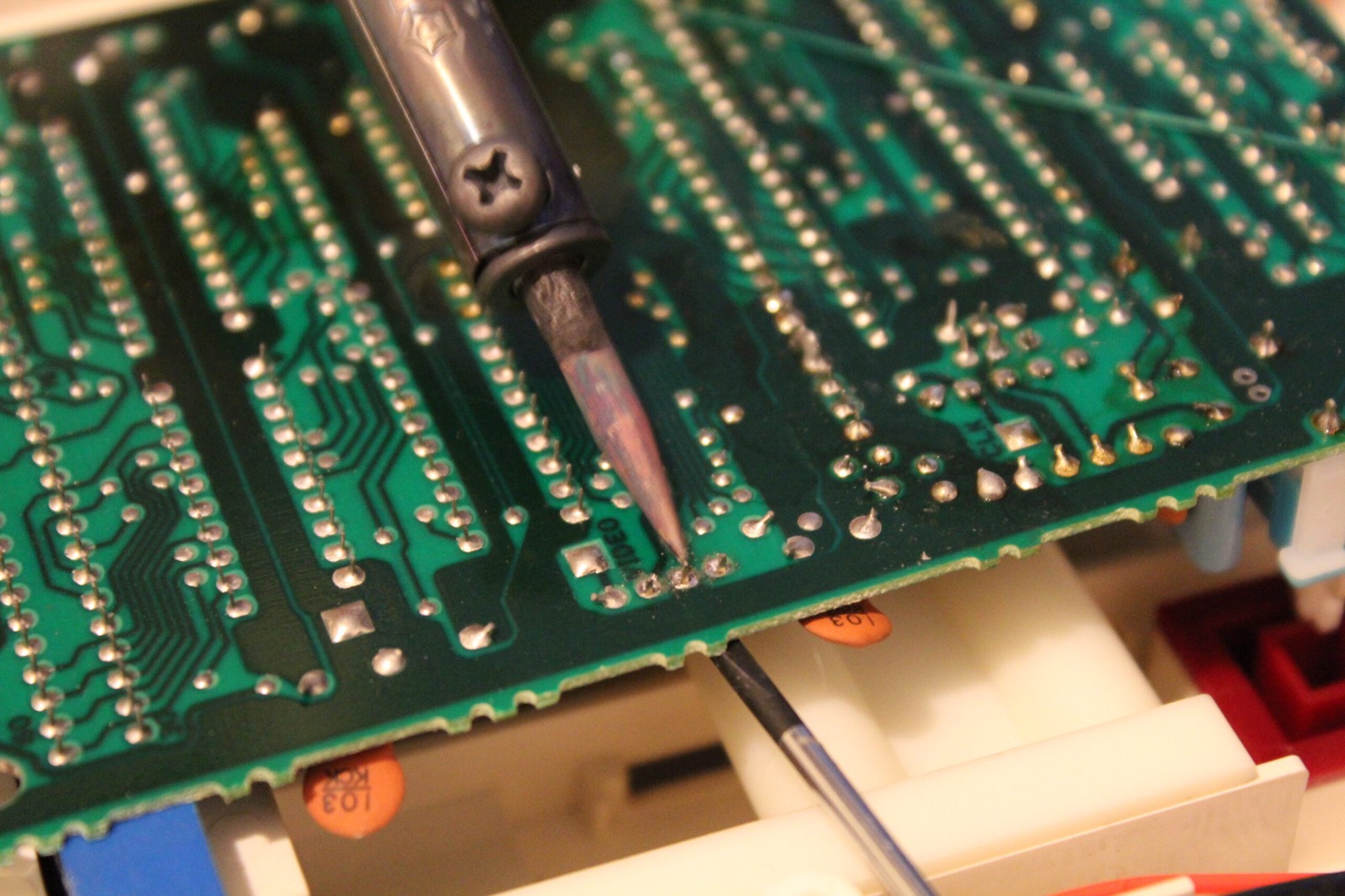 Desoldering the A937Q D PNP transistor from the Famicom mainboard.
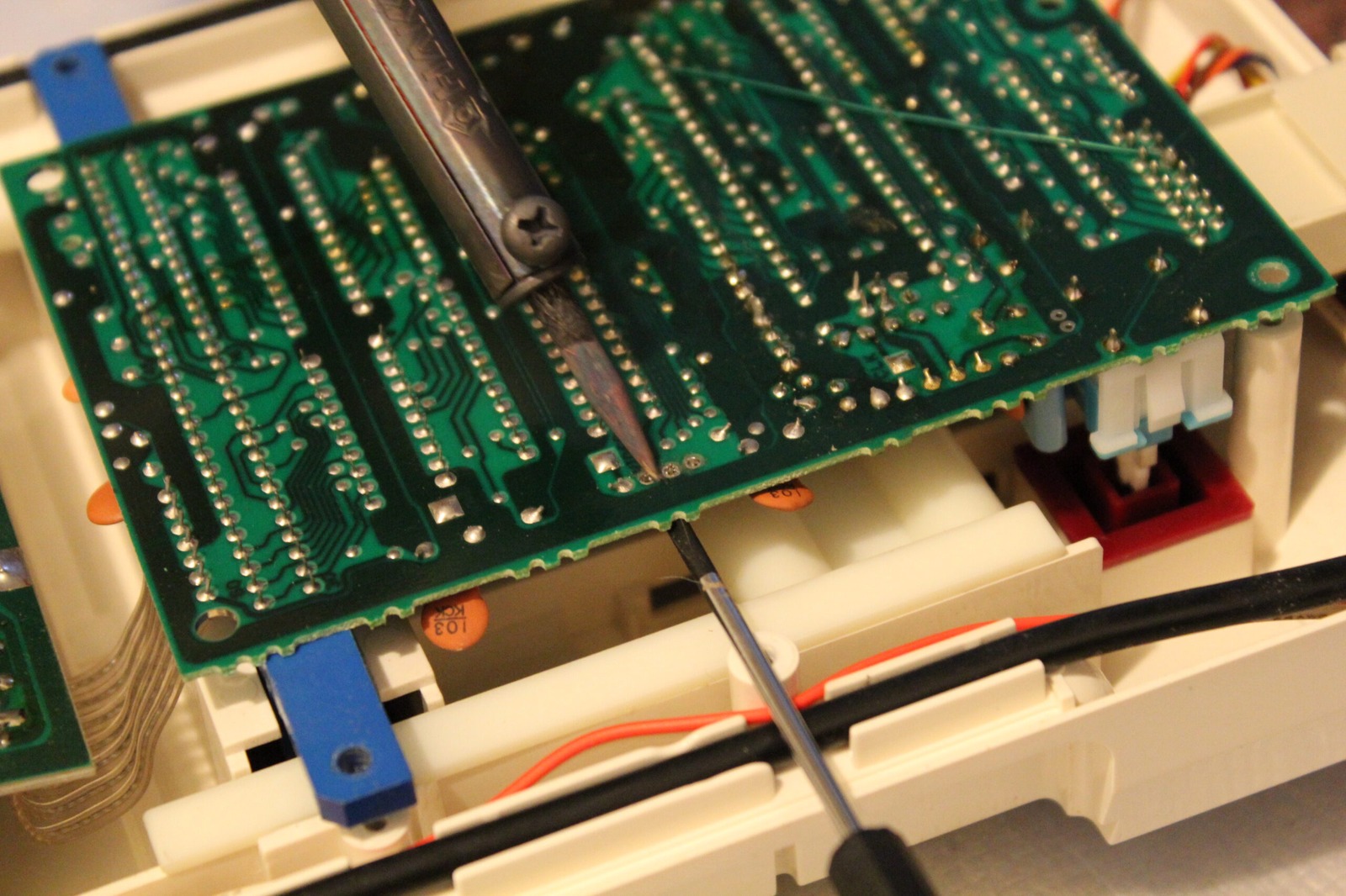 Desoldering the A937Q D PNP transistor from the Famicom mainboard.
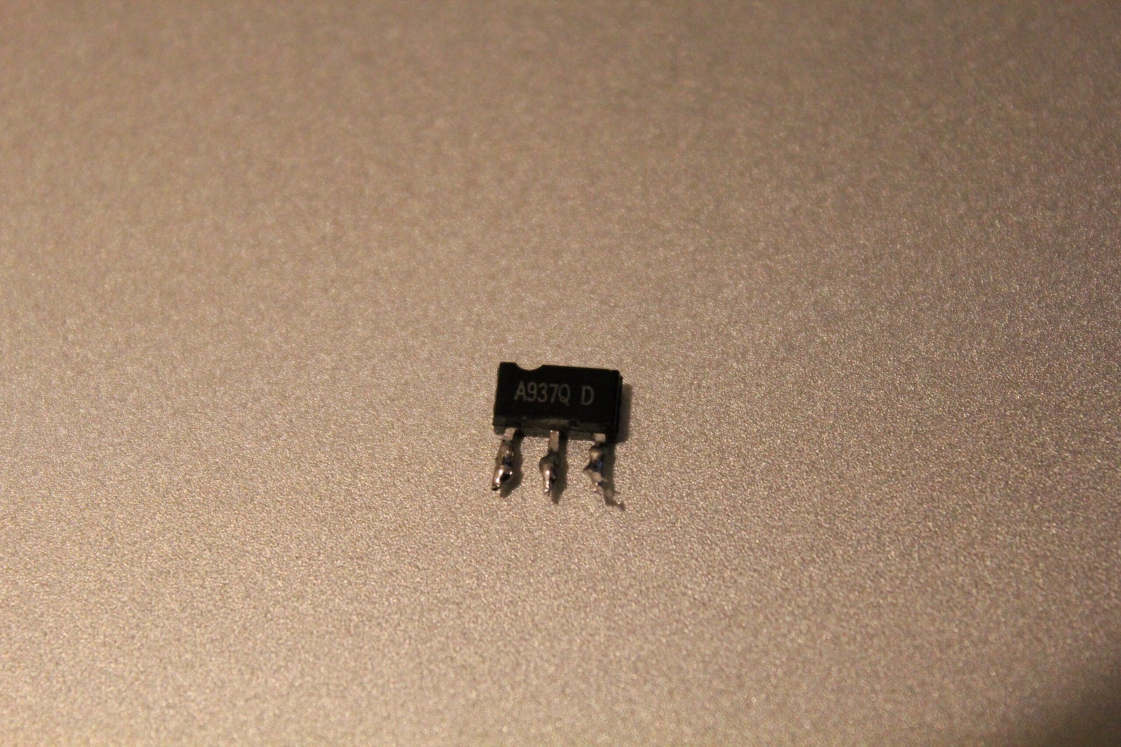 A937Q D PNP transistor desoldered from the Famicom mainboard.
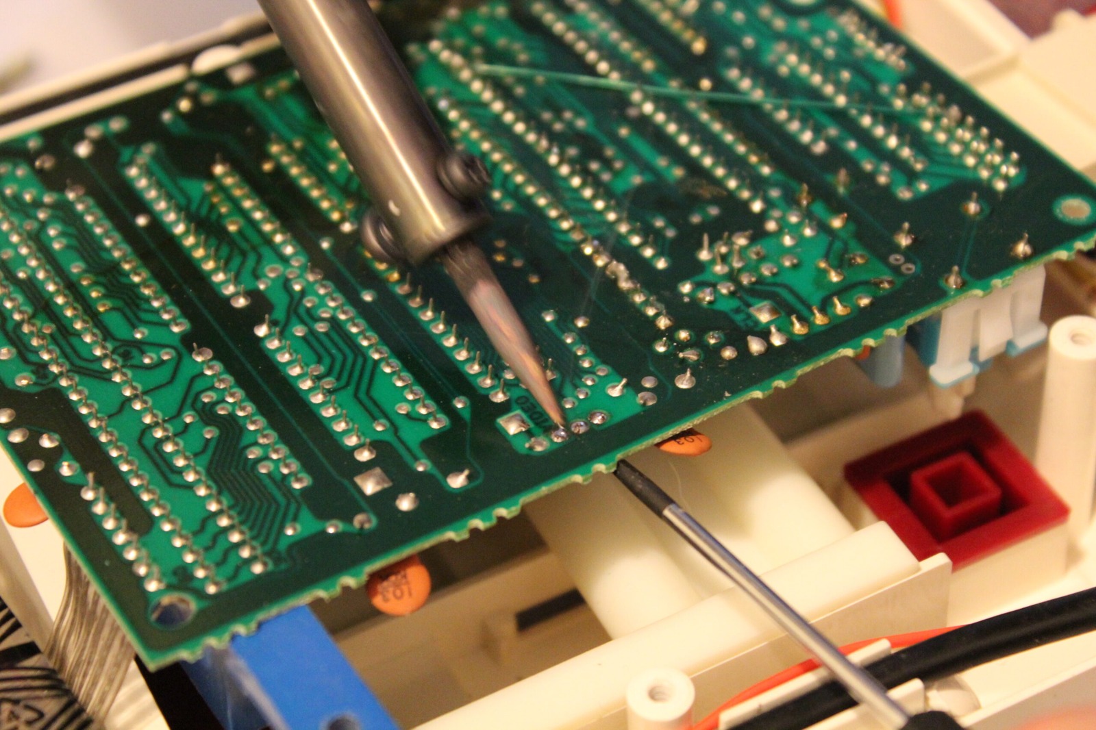 Desoldering the A937Q D PNP transistor from the Famicom mainboard.
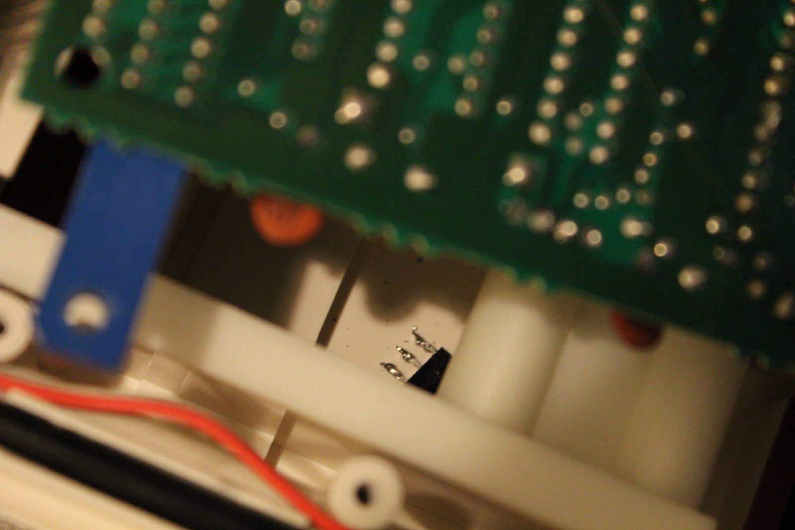 A937Q D PNP transistor desoldered from the Famicom mainboard. It fell into the Famicom…
Firstly, desolder the PNP transistor shown above from the mainboard. I originally used a small flatblade screwdriver to help lift it while heating the joints.
I would be gentler doing this now. A desoldering pump, braid or proper desoldering tool puts much less mechanical stress on an ageing PCB. The important thing is getting the component out without overheating it or lifting the pads.
Wiring the Famicom
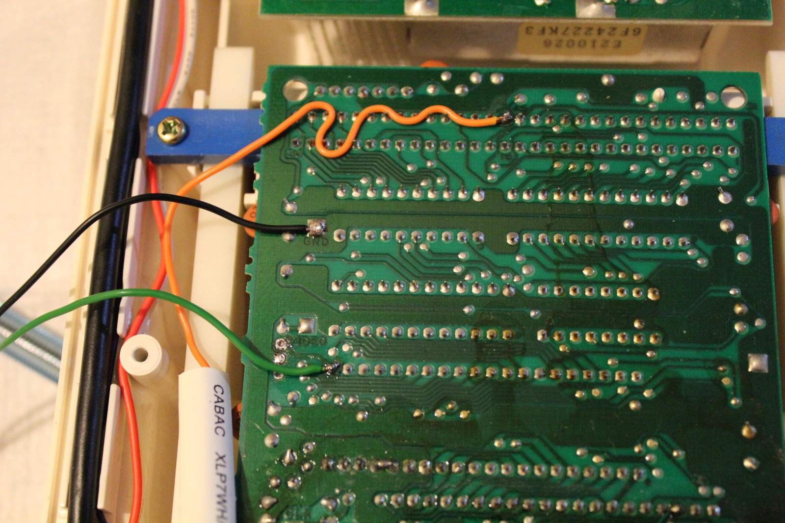
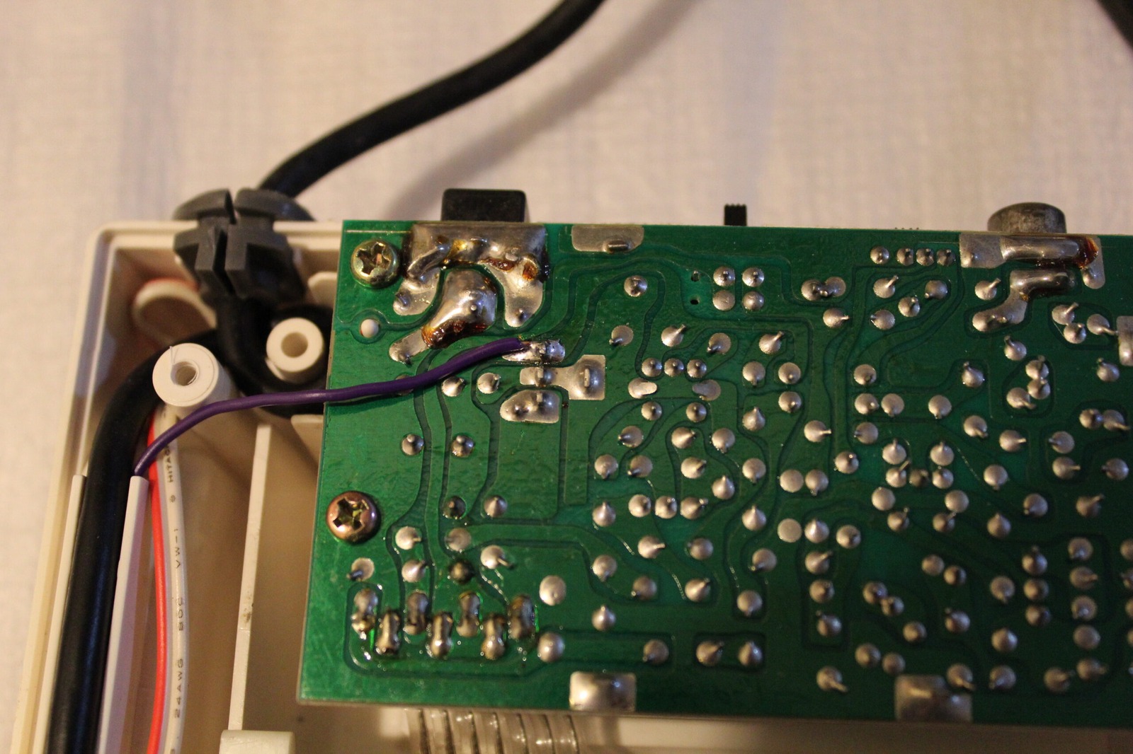
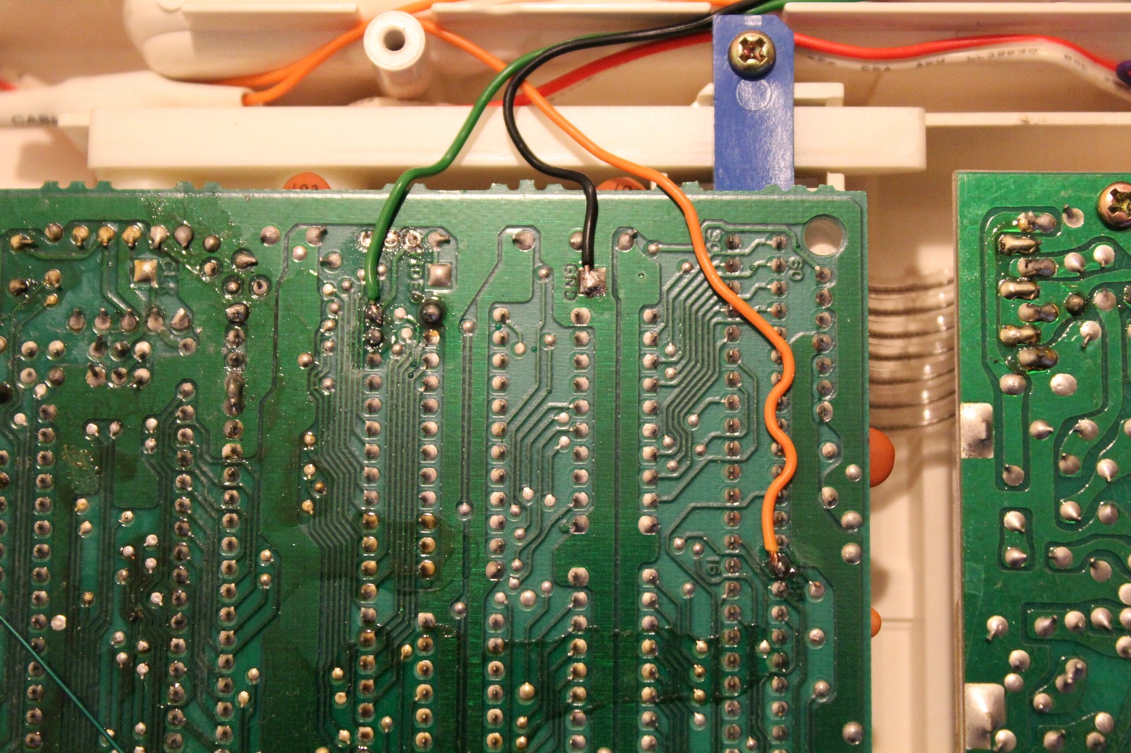
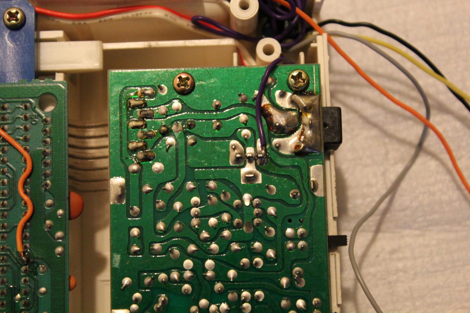
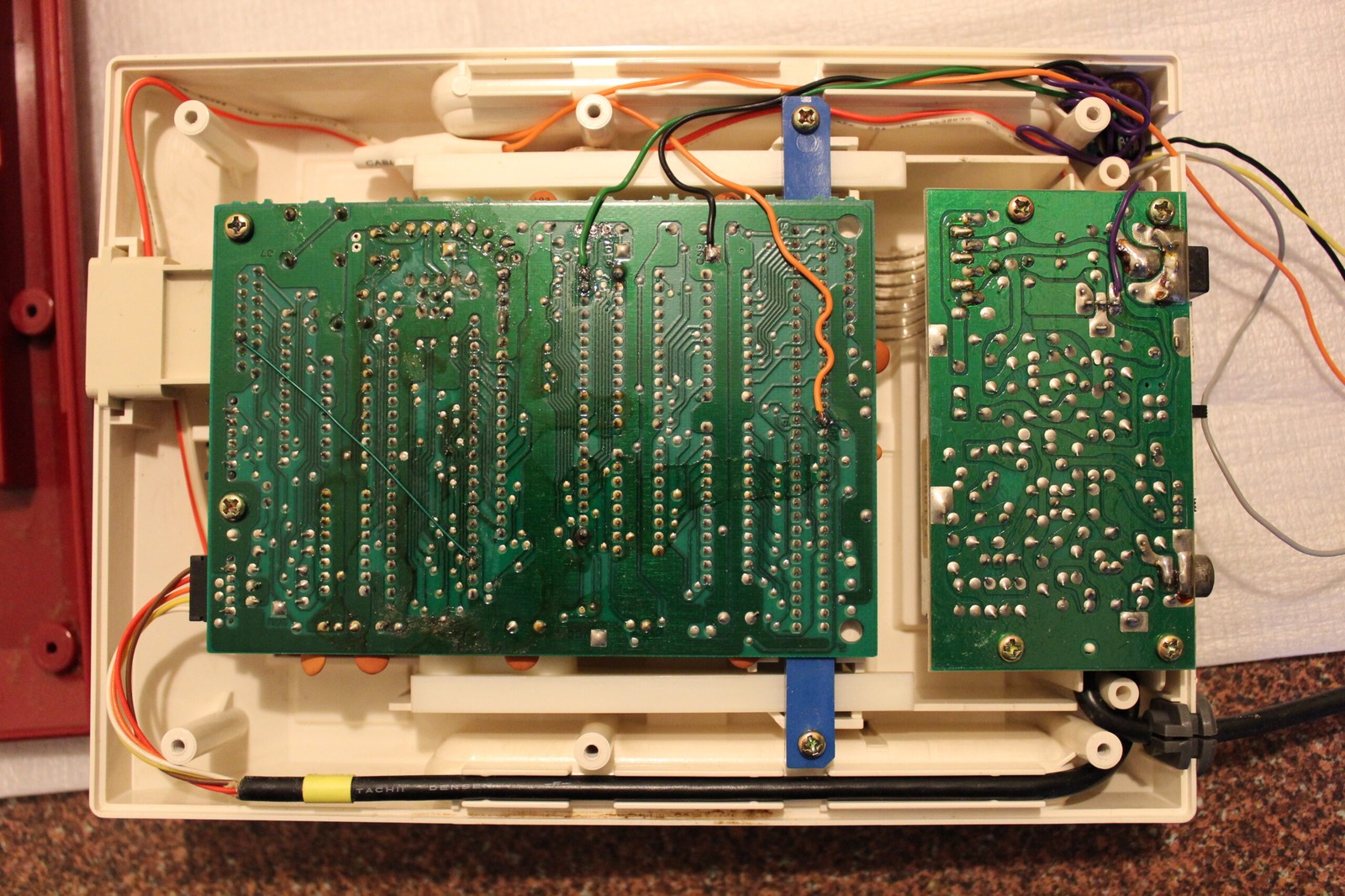
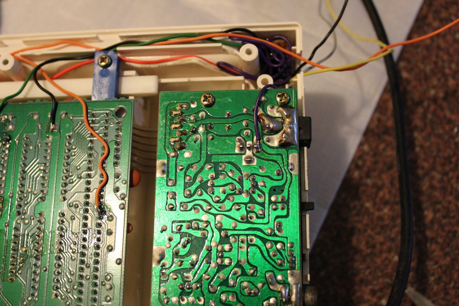
Next identify the four solder points required from the photos above. If your mainboard looks different, you have a different board revision. Sadly, I cannot help you with that one from these photos alone.
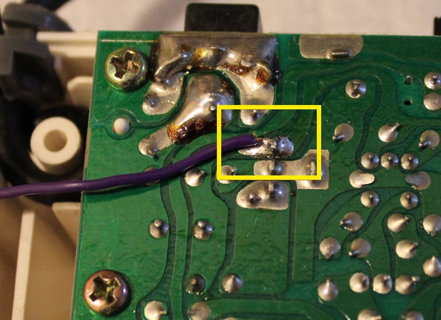 +5 V source
The purple cable taps into the voltage regulator, an LM7805, and provides the +5 V supply.
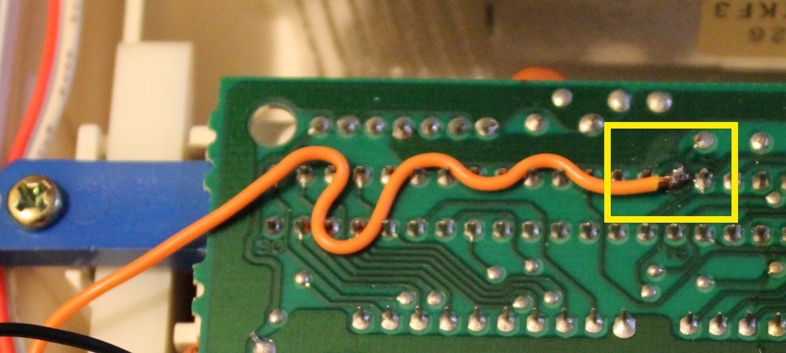 Sound
Sound
The orange cable is the audio signal source. The audio output also needs ground, which is the next connection.
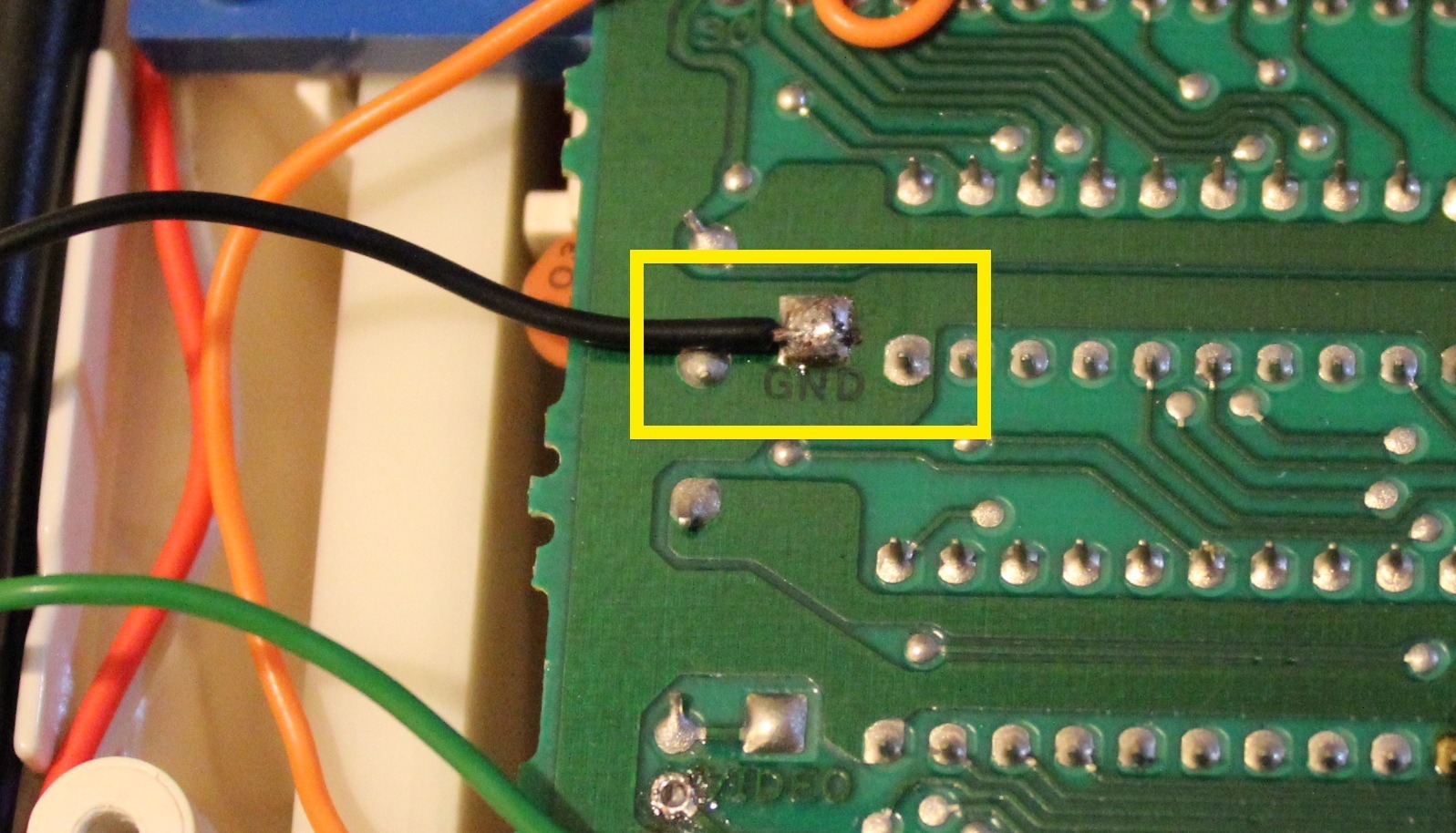 Ground
The black cable is the ground point. I ran a wire from it to the prototyping board and split it there for the other ground connections.
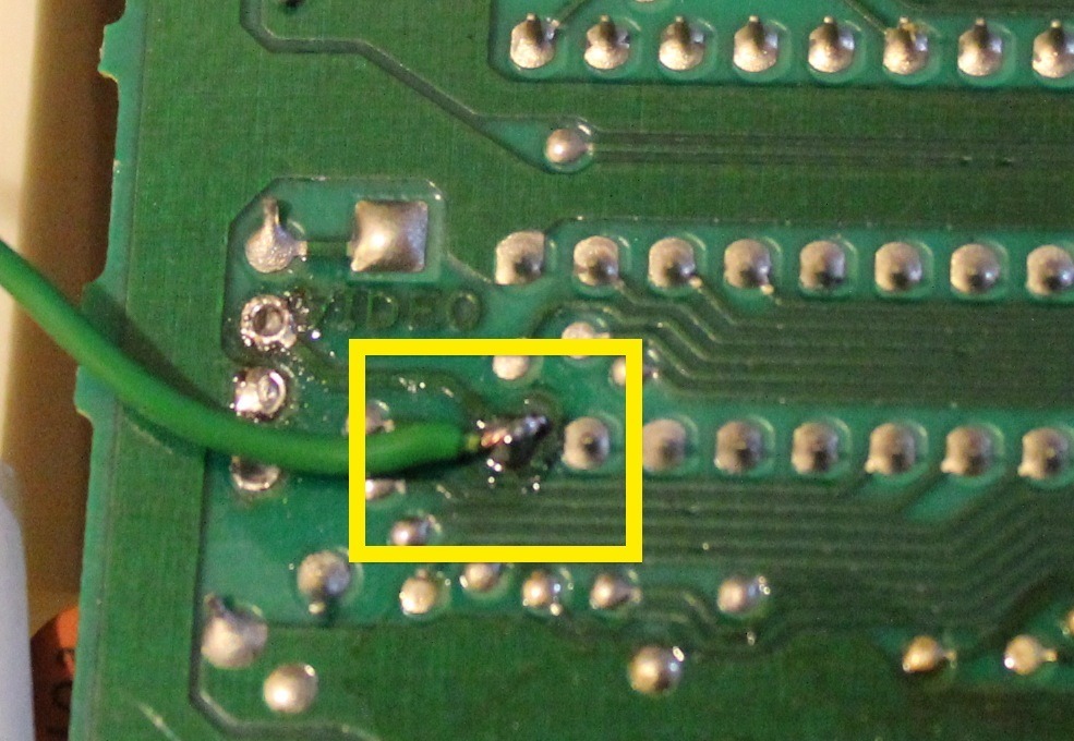 Composite video
The green cable is the composite-video signal. The RCA centre pin carries the signal and the outer connection goes to circuit ground.
Adding a little fresh solder and flux can make an old joint much easier to rework because it improves wetting and heat transfer. Melt the existing joint and add just enough fresh solder to get a clean connection.
I usually add enough that I don’t bother tinning the wires separately.
Yes… I know… lazy, isn’t it!
Building the composite board
Once the four wires are installed, grab the prototyping board. I cut mine down to size with whatever seemed appropriate at the time, including a knife, flatblade screwdriver and, once, a hacksaw.
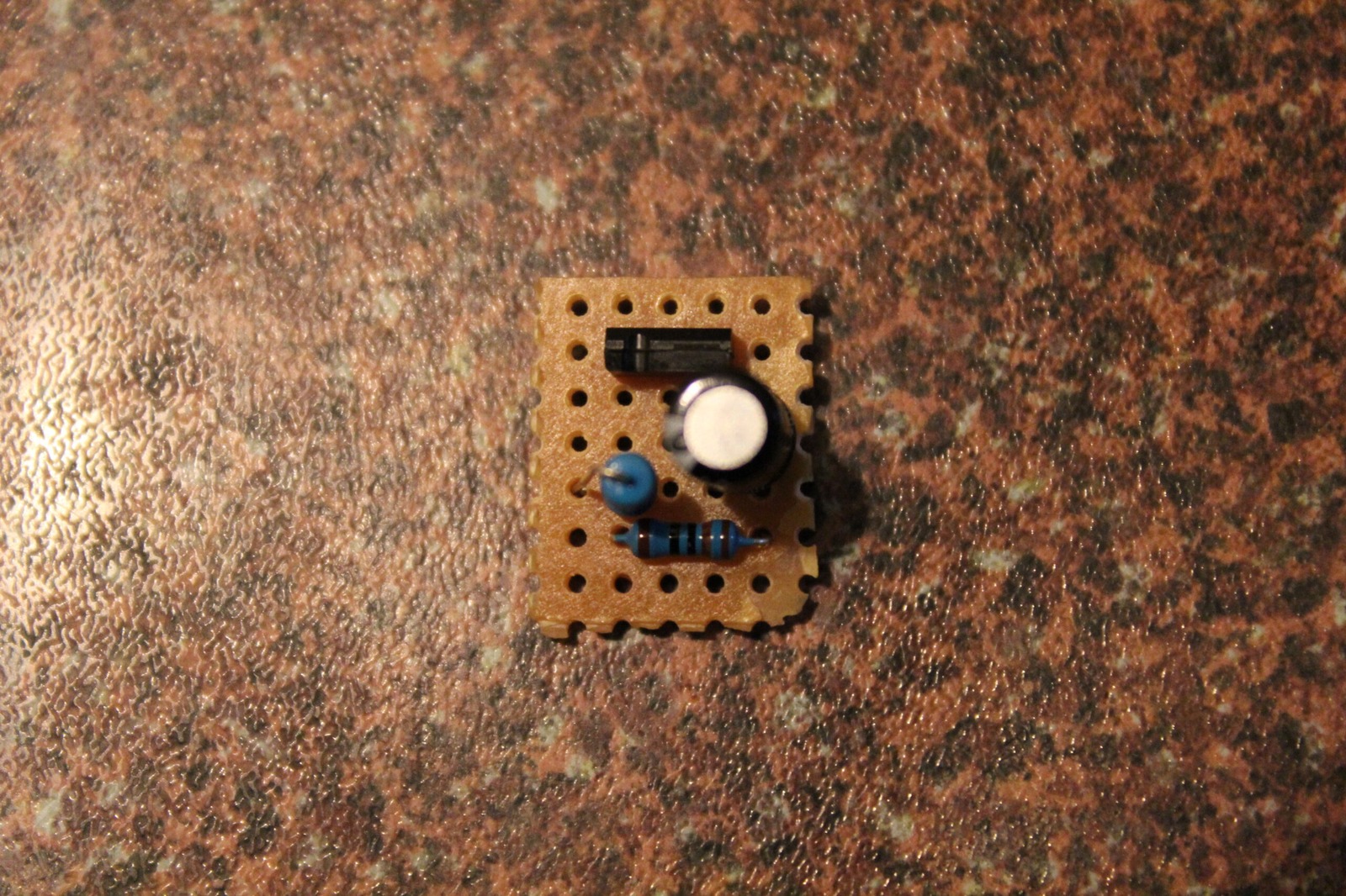
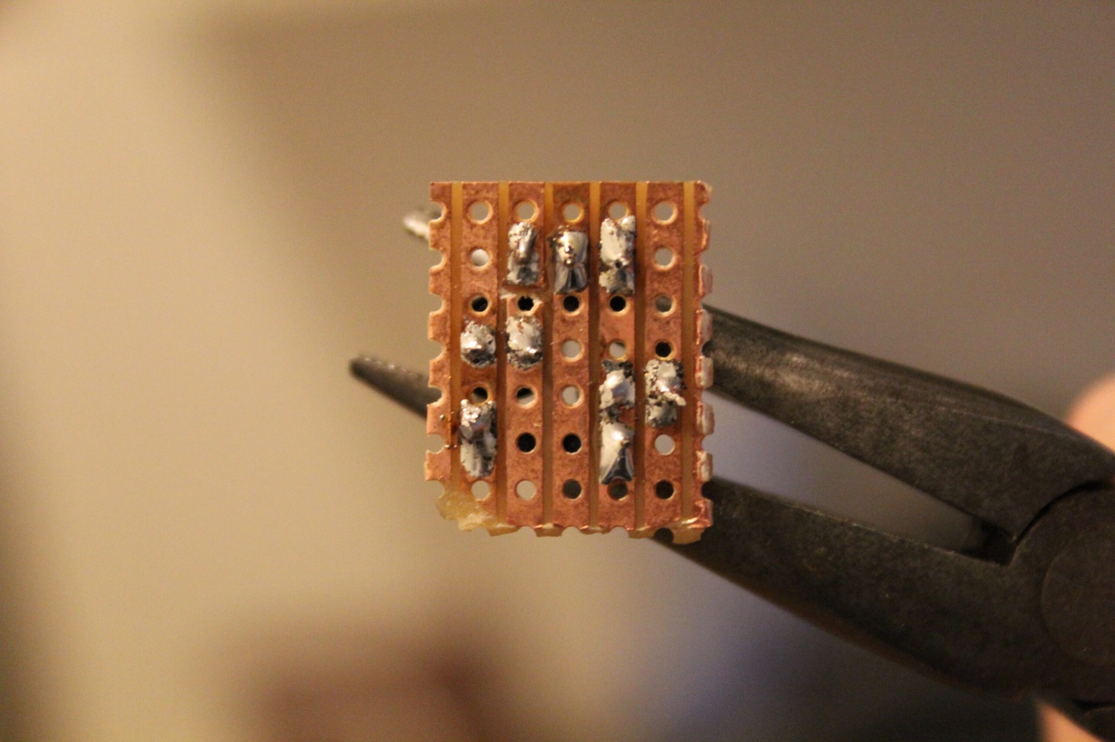
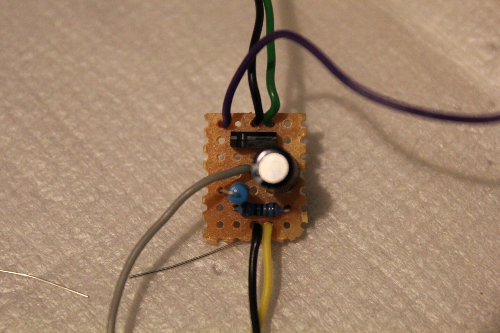
The board I used is 5 x 7 holes. The photographs show the layout I built.
Resistors are not polarised, but the electrolytic capacitors are. Make sure their polarity is correct.
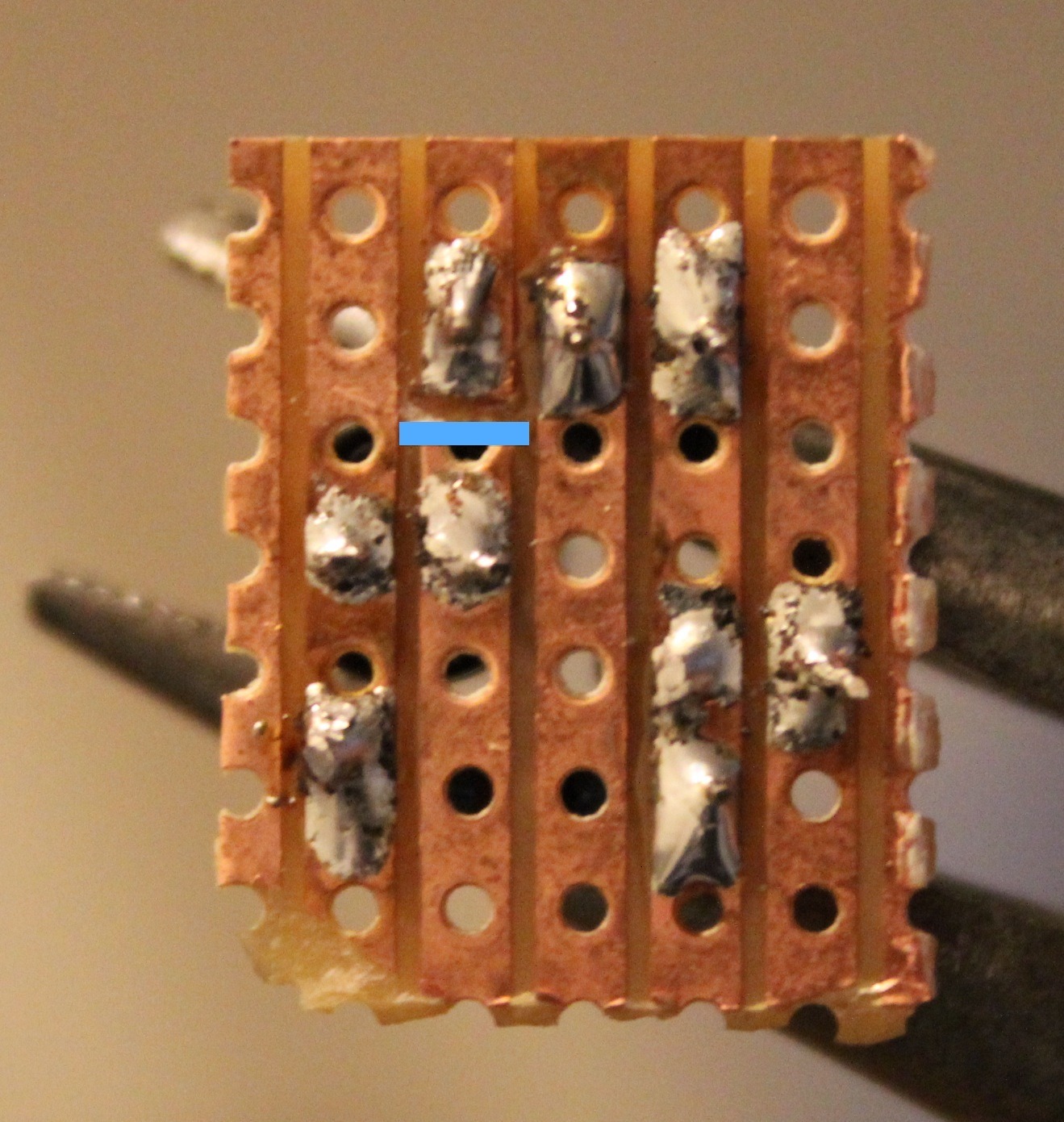 Cut this track on your prototyping board
The copper track shown above has to be cut so the circuit sections are isolated correctly. I scraped through it with a flatblade screwdriver.
Use a multimeter to make sure there is no continuity across the cut before powering the circuit.
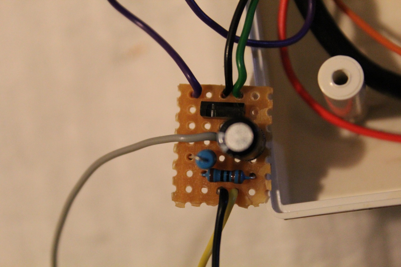
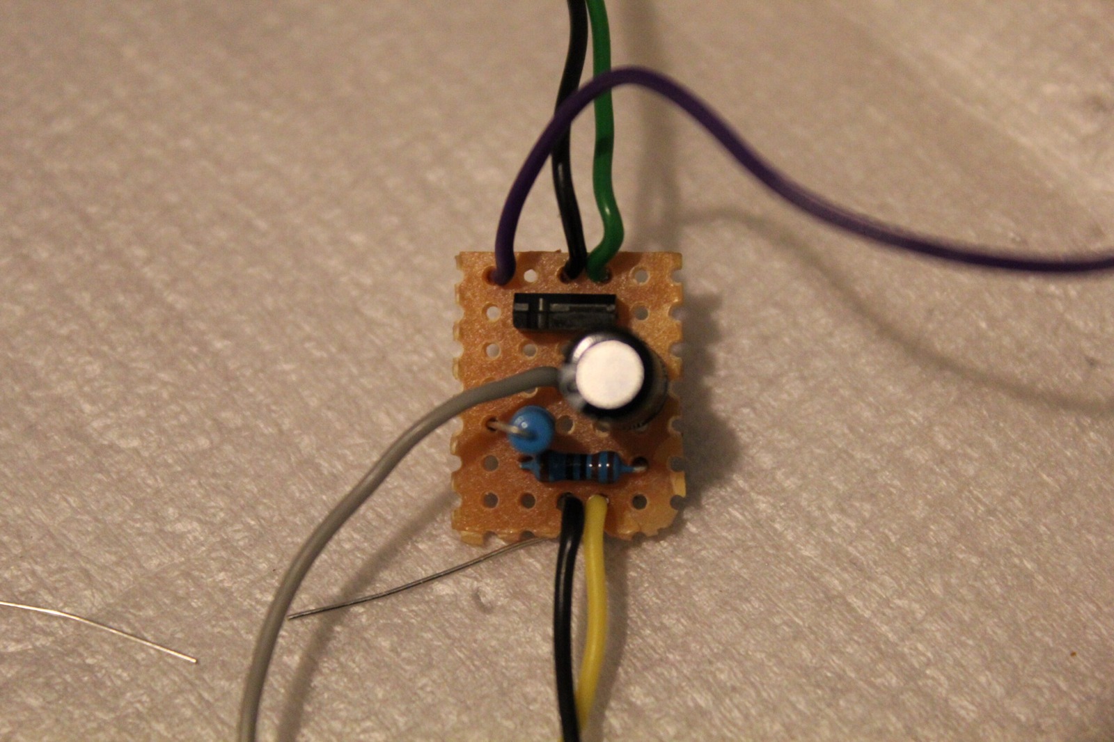
The cable colours in my build are:
- Purple: +5 V from the LM7805
- Green: composite video from the mainboard
- Black and grey: ground
- Yellow: composite video output to the RCA centre pin
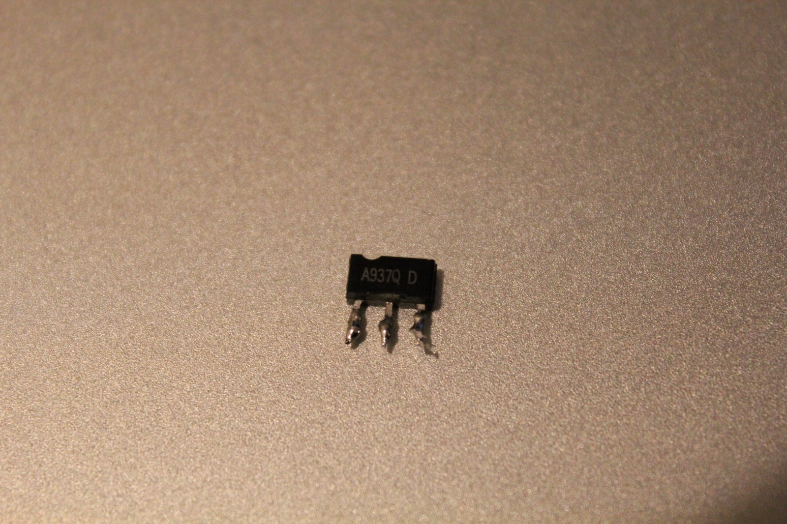
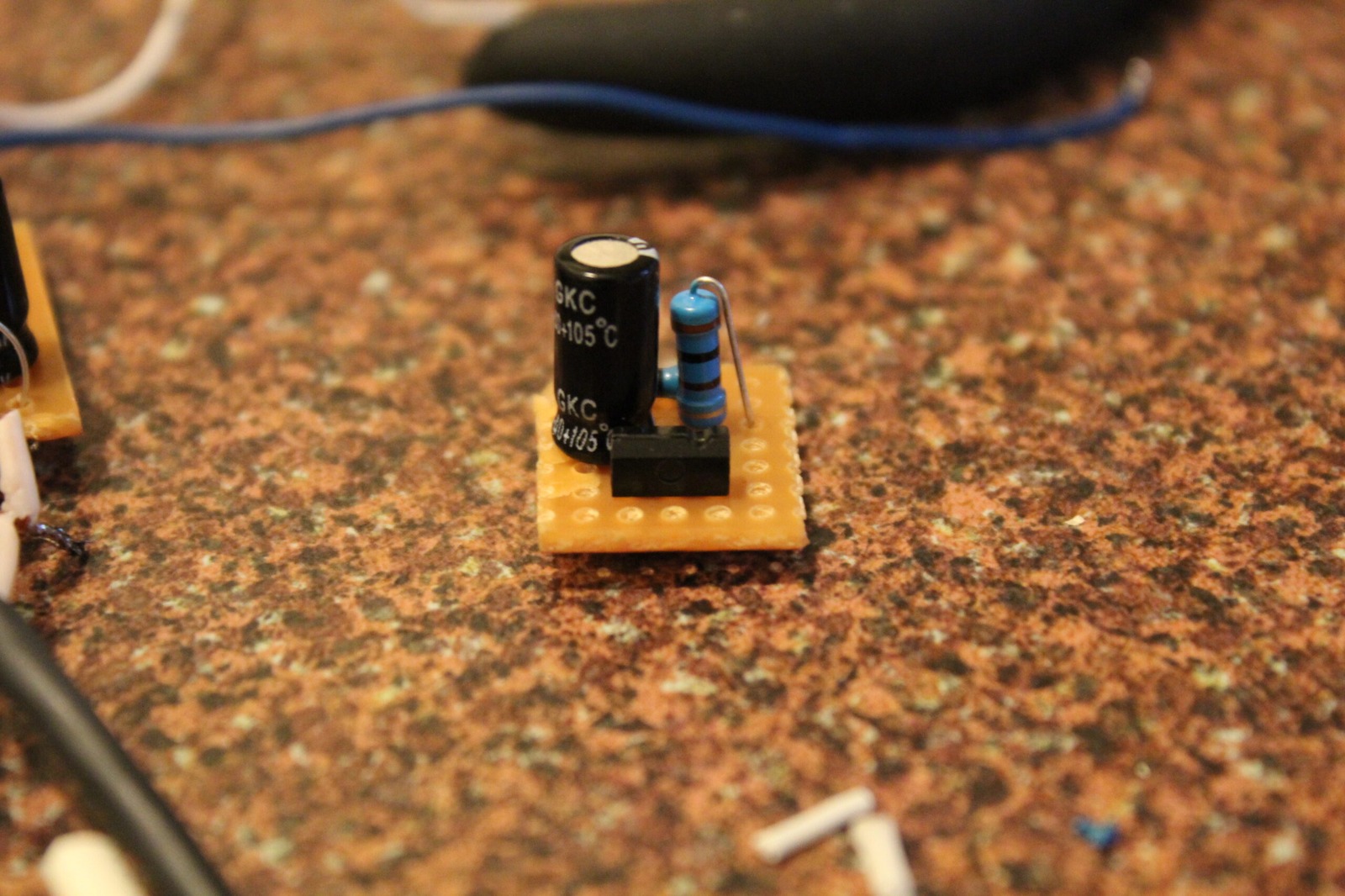
Make sure the transistor goes back into the new circuit with the correct emitter, collector and base orientation. If the modification does not behave as expected, switch the console off and disconnect the power adaptor before checking the wiring, transistor orientation and capacitor polarity.
Audio output
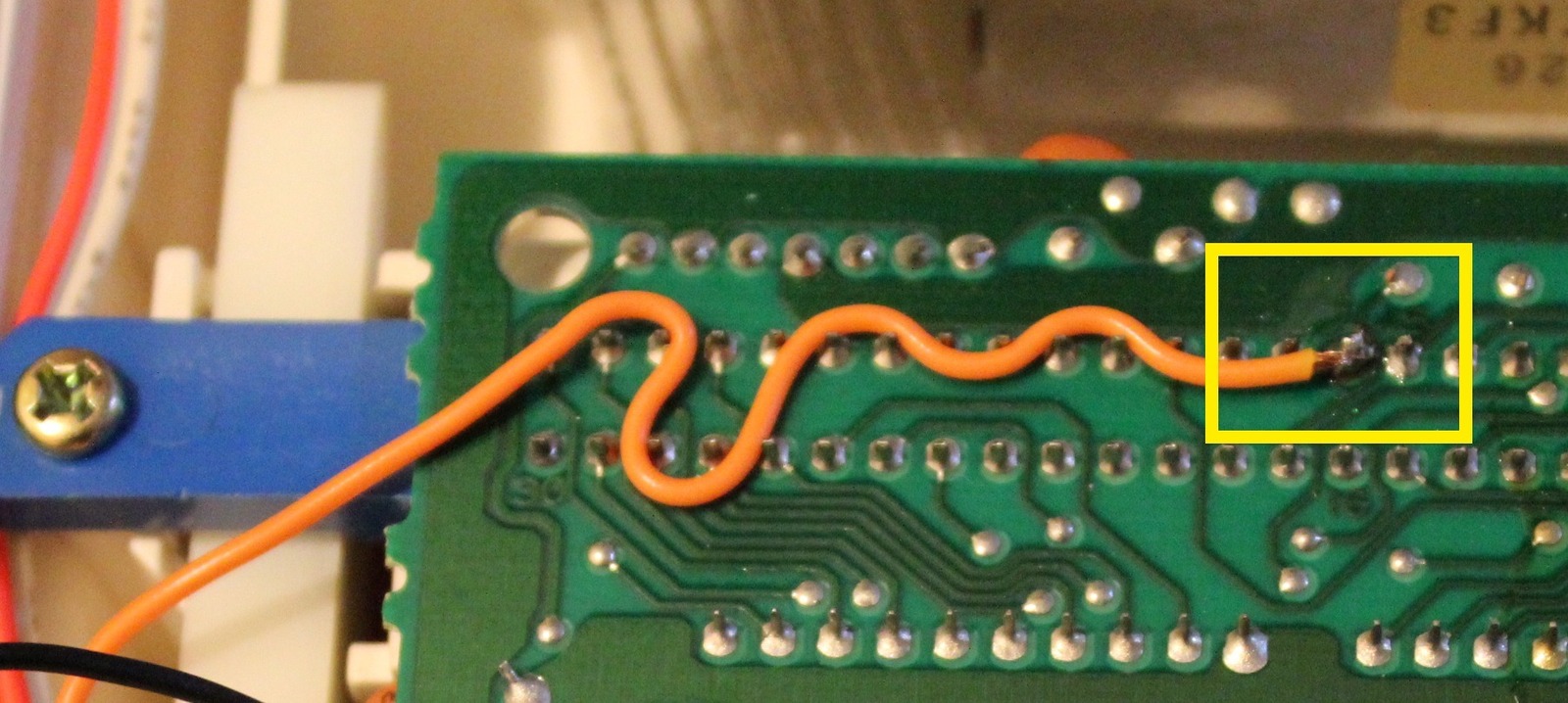
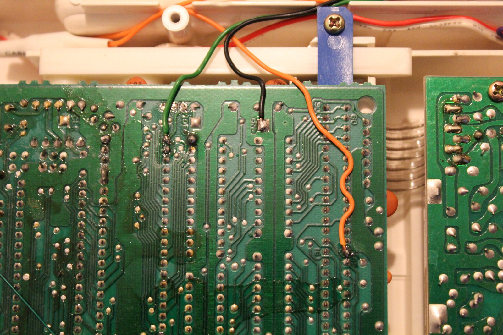
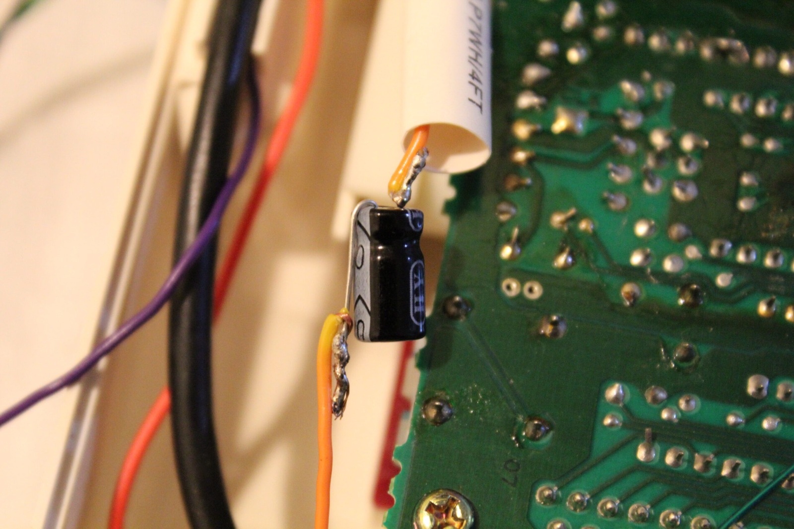
The orange audio wire shown in the photographs runs into a 220 uF, 16 V electrolytic capacitor. In this build the positive side faces the mainboard and the negative side leads to the centre pin of the audio RCA socket.
Add a ground connection and that completes the audio output. Again, make sure the electrolytic capacitor polarity is correct.
Finished result
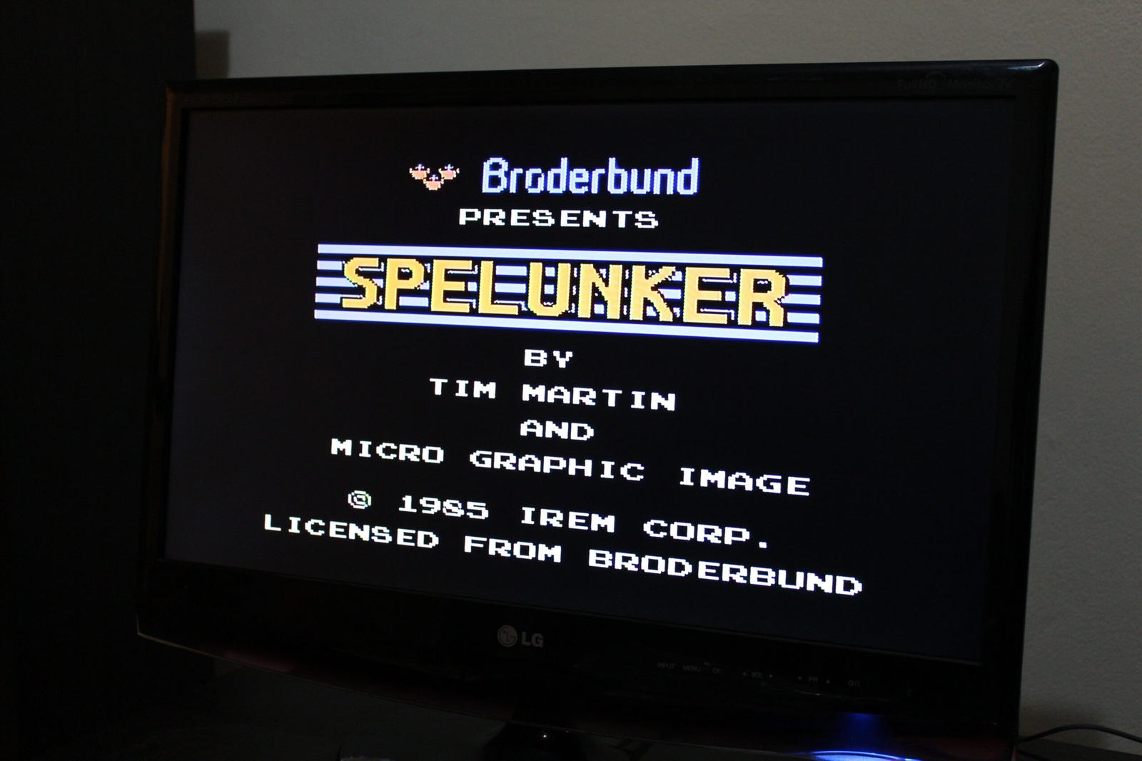
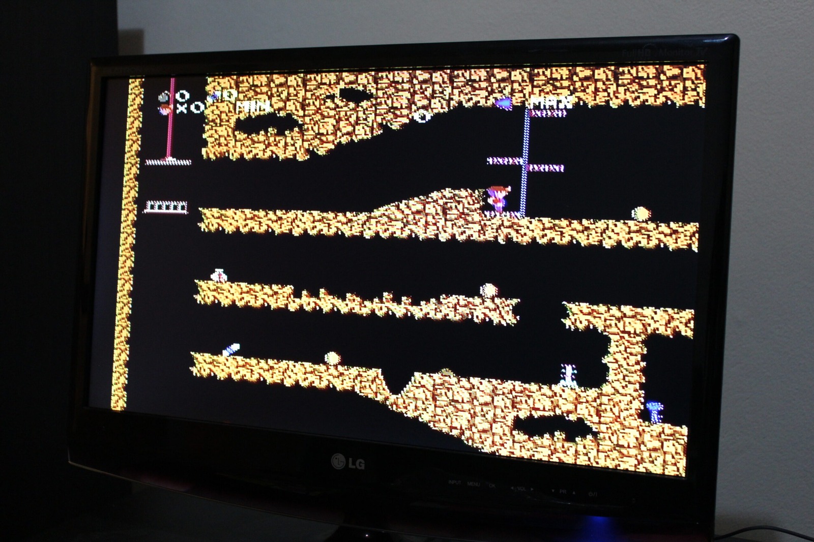
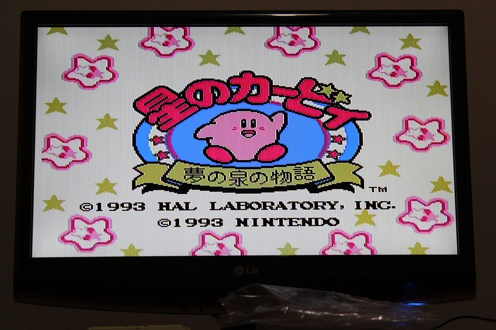
Now all that’s left is to enjoy Kirby and Spelunker!
Below are some videos of the unit while it was in pieces, explaining where the wires run and how this particular build went together.
A later guide covering improved Famicom AV modification and jailbar-reduction techniques can be found in JPX72 - Famicom AV mod - NEW!. It documents a related approach and useful schematics. I had no luck with the jailbar-reduction methods I tried. Your luck may vary. Good luck!
Related posts
Resources
Sources
- JPX72 - Famicom AV mod - NEW! - a later guide, published in 2016, covering Famicom AV modification and jailbar reduction.
- ConsoleMods - NES Top Loader AV Mod - documents a closely related PNP-transistor composite amplifier topology used in Nintendo RF-only hardware.
- Ctrl-Alt-Rees - Nintendo Famicom Composite Video Output Mod - documents Famicom board-revision differences and later composite-mod approaches.