 Nix McRetro
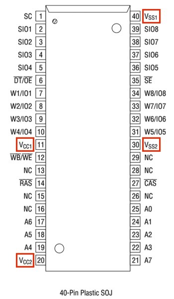
After actually reading the RAM datasheet properly, I realised that disturbing the power pins might explain some of my earlier random resets. On the 40-pin SOJ pinout shown here, VCC is on pins 11 and 20, and VSS on pins 30 and 40. Those are not pins I want to be casually shorting or disturbing during circuit-bending experiments.
The useful lesson is simple: identify the signal pins from the datasheet first and keep the power and ground pins out of the experiment. Blindly poking neighbouring IC legs is an excellent way to turn entertaining video corruption into dead RAM.
I’ve updated the earlier Mega Drive circuit-bending post to make that distinction clear too. Next I’d like to make a video, or maybe several, on getting the best visual artefacts the Mega Drive can offer without sacrificing perfectly good hardware.
