 Nix McRetro
I finally got around to doing some soldering on a somewhat faulty Mega Drive 2 I had lying about. I started from the old gieskes.nl circuit-bending diagram, but after checking the VRAM pinout properly I deliberately stayed away from the VCC and VSS power pins.
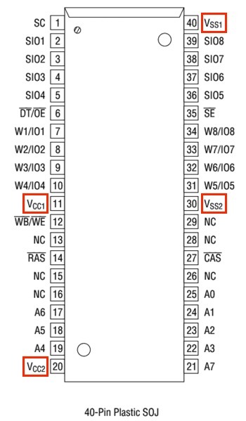
On the VRAM I concentrated on address inputs, grounding them to get results. The pinout above labels them A0 through A7; my original A0-to-A8 description went one address line too far. Interfering with those signals can produce wonderfully broken graphics. This is deliberately abusive experimentation, not a repair technique, and neighbouring pins should not be assumed safe just because they are close together.
Then I started messing with the Z80 RAM, particularly address lines A8, A9, A10 and A11, and whatever /OE is. Possibly with a dash of /CE1. Those last two are control signals, not address lines.
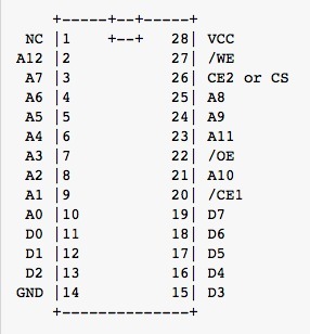
Messing with the data lines tended to hang the console and require a power cycle. Plenty more address lines to play with there, though. I’ve decided to put circuit bending over on the McRetro Gaming YouTube channel since technically it’s some sort of gaming. I’ll be doing one of these a week if I remember and people show enough interest in staring at all the pretty patterns and odd sounds. It will be very interesting to see what each game can do.
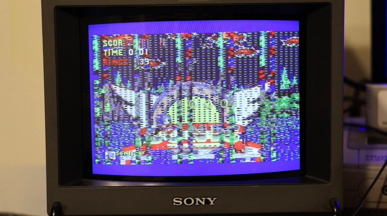
Big thanks to Console5 for the pinout reference.
Sources
- Gijs Gieskes - Personal Home-Page (archived)
- Sega - Genesis II / Mega Drive II Service Manual, 1993 supplements