 Nix McRetro
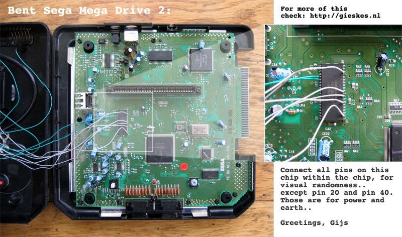
Gijs’ Mega Drive 2 circuit-bending diagram. Some gloriously broken graphics are possible, but the original note leaves out other power pins, so don’t follow it blindly!
Here’s a little infographic on circuit bending the Mega Drive / Genesis Model 2, originally from Gijs at gieskes.nl.
You can get some wonderfully broken graphics out of the VRAM. Maybe I should do another video - if only it also broke the audio… actually, I did mess around with address / data lines around the audio hardware on a Mega Drive Model 1, but it froze every so often.
Update: One important correction to the original diagram: it excludes only pins 20 and 40, but the VRAM has multiple VCC and VSS power pins. Those are not circuit-bending targets. Do not blindly bridge pins together. Verify the pinout of the actual RAM fitted and keep experiments away from power and ground unless you particularly enjoy converting vintage hardware into smoke.
We’ll come back to this with a more careful VRAM-specific experiment later.
