 Nix McRetro
While looking into the Sega TeraDrive Model 2, I came across a fascinating Japanese look inside IBM’s PS/55 Type 5510. It is one of those machines that looks familiar at first, until you start paying attention to the motherboard and cables. There is some wonderfully peculiar hardware in here!
The photographs and hands-on observations below come from Schwarzschild Cafe / FunkyGoods’ article published on 21st February 2010, part 32 of the author’s Decadent PC-Compatible Hobby series. This is a newly edited English-language adaptation and technical summary, not my own teardown or a word-for-word translation. I’ve kept the original sequence of images and some of the author’s sense of humour, while distinguishing observations from guesses and preserving the technical cautions already added to this post.
Inside the PS/55 Type 5510

The PS/55 Type 5510-Z02 with the case removed. The long enclosure across the top is its power supply. This particular configuration has two floppy drives and no internal hard drive.
The Japanese author describes opening the case of an IBM-made PS/55 Type 5510, then taking a close look at what is inside. It is an original IBM PC/AT-compatible design, but the motherboard has little in common with the conventional Baby AT boards found in many other computers of its era. Rather than relying on a collection of expansion cards, IBM put serial and parallel I/O and VGA video on the motherboard itself.
The ISA expansion slots sit on a riser card rather than directly on the main board. There are only three, but with so much already built in, that is not necessarily a problem. The author also has a laugh at the expense of this long-running vintage-PC series: there may not be much practical value in dismantling another obsolete machine, but that has never stopped a dedicated hardware enthusiast!
What is on the motherboard?
This is a 12 MHz 80286-era system. Its functions are distributed across a considerable number of separate chips, with Western Digital supplying much of the support logic. The major devices identified in the Japanese article are:
| Chip | Identification in the source |
|---|---|
| Intel N80286-12 | 12 MHz 80286 CPU, PLCC package |
| Intel C80287XL | Optional maths coprocessor |
| Western Digital WD76C10LP-LR | System controller |
| Western Digital WD76C20-JU | Floppy disk controller |
| Western Digital WD76C30-JU | Serial/parallel I/O and clock-generation functions |
| Western Digital WD90C10-LR | VGA controller |
| Intel iP8042AH | Keyboard controller |
| Inmos IMSG176P | 6-bit video palette DAC |
| IBM 79F2661 | Unidentified; the original author suggests it may be related to hard-disk control |
The article describes chips dated to the latter part of 1990 and an IBM-branded onboard memory arrangement. Four 30-pin SIMM sockets provide additional memory expansion. They were empty when the author acquired the machine, but suitable modules from their collection were recognised when fitted.

An overview of the motherboard. The long connector near the centre accepts the ISA riser. A standard CR2032 battery handles CMOS retention, which is rather convenient for a machine of this vintage. The author also found a 3rd April 1991 date stamp inside the case.

The 12 MHz 80286 and the optional 80287 coprocessor. The coprocessor’s ceramic package and gold lid are particularly striking. A hand-added jumper wire is visible nearby.

IBM-branded onboard RAM alongside the 30-pin SIMM sockets. The photograph also shows the WD76C10 system controller and Intel 8042 keyboard controller.

The WD76C30 handles serial/parallel I/O and clock-related duties. The WD90C10 VGA chip, video memory and DAC are also visible. That colourful ribbon cable will become important shortly.
Jumper wires and curious drive connectors
The author noticed a surprising amount of jumper wiring on this board. On a production motherboard, that kind of handwork looks time-consuming, and the article wonders what it added to the cost of building the machine.
More interesting still are the drive connectors. A typical PC-compatible floppy interface uses a 34-pin cable, while a conventional desktop IDE hard drive generally uses 40 pins. The PS/55 motherboard in this article instead has a 40-pin floppy connector and a 44-pin hard-disk connector.
Does that mean the floppy drive itself is unusual? Apparently not. The actual drive has the familiar 34-pin connection. The additional six positions are on the motherboard end of the ribbon cable, where the source photographs show them unused. The original author suspected there might be a similar arrangement for the hard-disk connection, but did not establish that as fact.
The article also considers whether the extra pins might have been reserved for three-mode floppy-drive signals. That is a theory, not a confirmed explanation. Why IBM chose this arrangement remains an interesting little mystery. What sort of enthusiast wouldn’t want to know?

Detail of the wiring around the system controller. The handwork is unusually prominent for something that otherwise looks like a neatly engineered production motherboard.

The ISA riser has three expansion slots, reinforcing the machine’s PC/AT-compatible design.

With the riser fitted, the system can accommodate three full-length ISA expansion boards.
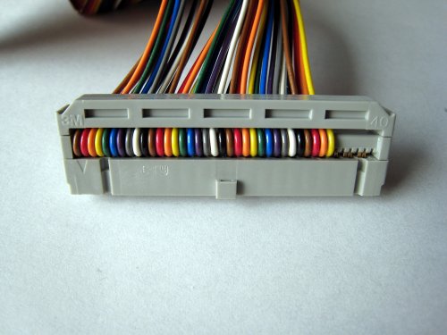
The unusually wide motherboard-side floppy header, compared with the 34 conductors actually used by the drive cable. The six extra positions are visible at one end.
A familiar Western Digital design

The original author found a WD76C20 floppy-controller block diagram whose overall arrangement resembled the PS/55 motherboard. The video DAC was one noted difference. This is a design comparison, not proof that every circuit follows the reference exactly.
With the system controller, floppy controller, serial and parallel functions, and VGA all provided by Western Digital chips, the board starts to make more sense. It is also a good reminder of just how many individual parts were needed to implement what later machines would integrate into far fewer devices.
How does it compare with an IBM PC/AT?

An IBM PC/AT Type 5170 motherboard, included in the Japanese article as a comparison. The older design has a very different layout and lacks the PS/55’s integrated VGA and serial/parallel functions.
The original article labels the comparison as a 1984-era PC/AT motherboard with an 8 MHz 80286. That wording needs some care: IBM’s own product reference distinguishes the 6 MHz 5170-068 from later 8 MHz models such as the 5170-319 and 5170-339. The image is still useful as a visual comparison, but the exact model should not be inferred from the caption alone.
The price, and one more mystery
According to the Japanese article, the basic PS/55 5510-Z02 originally cost ¥198,000, which the author regarded as exceptionally inexpensive for an IBM-branded computer at the time. A configuration with a 40 MB IDE hard drive was also available, but the author did not know its original price.
And naturally, that is not the end of the story. The article finishes by teasing a particularly strange expansion card for the next instalment. If an unusual floppy cable and all those jumper wires weren’t enough, apparently there was more to come!
Sources
- Schwarzschild Cafe / FunkyGoods - Decadent PC-Compatible Hobby, Part 32: PS/55 Type 5510 Disassembly (21st February 2010), original Japanese article
- Schwarzschild Cafe / FunkyGoods - Part 31: Discovering the PS/55 Type 5510 (23rd January 2010), original Japanese article
- Schwarzschild Cafe / FunkyGoods - Part 33: The Mysterious Hard Disk Card (27th February 2010), original Japanese article
- IBM - Personal System/2 and IBM Personal Computer Product Reference, Version 4.0 (April 1987), page 49
Related Posts