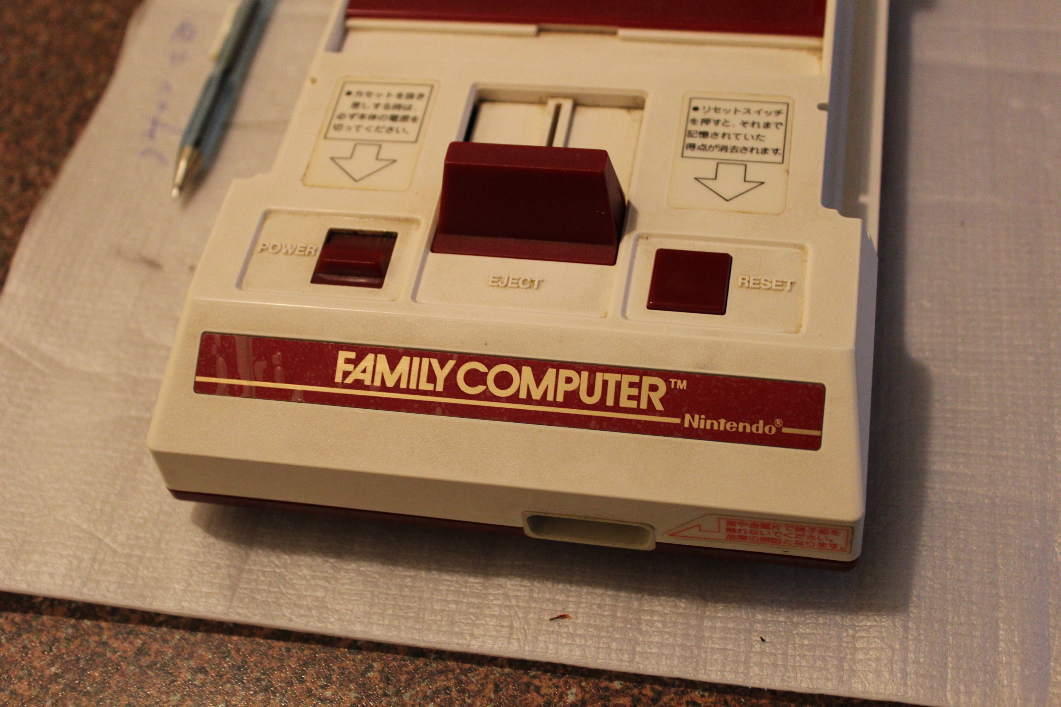
The Nintendo Family Computer. Ohhhh yeahhhh! Below are the first, second and third revisions of my attempt at an AV mod for the Famicom.
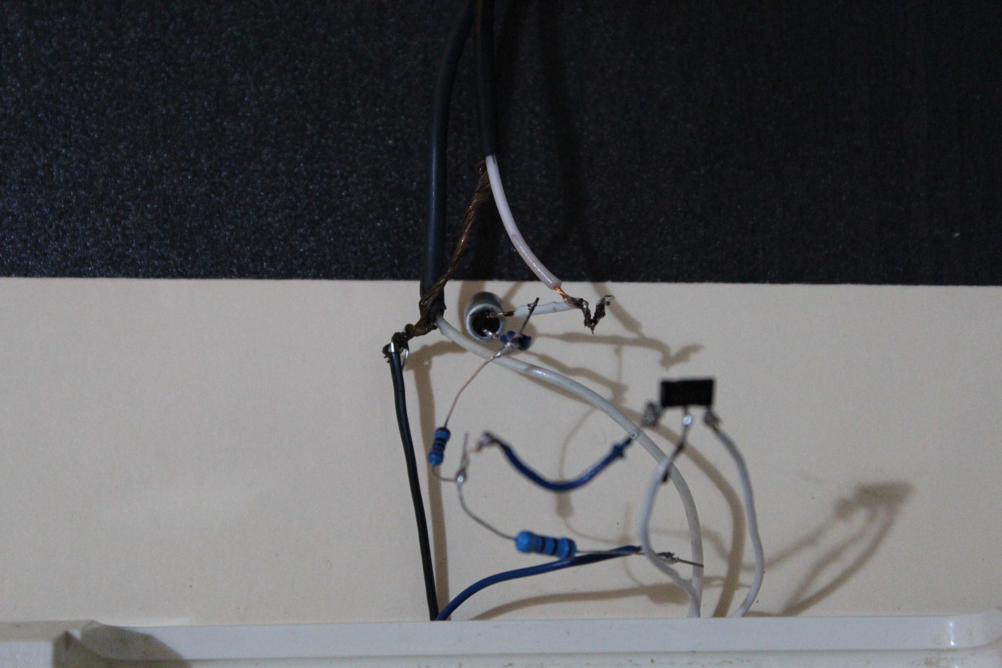
The first attempt was a proof of concept, hence the mess of cables – functional yet hideous.

The second attempt is the slightly longer prototyping board. I was attempting to build it using sub-par parts such as a cable tie as a wire for ground. While it worked, it was not what I wanted.
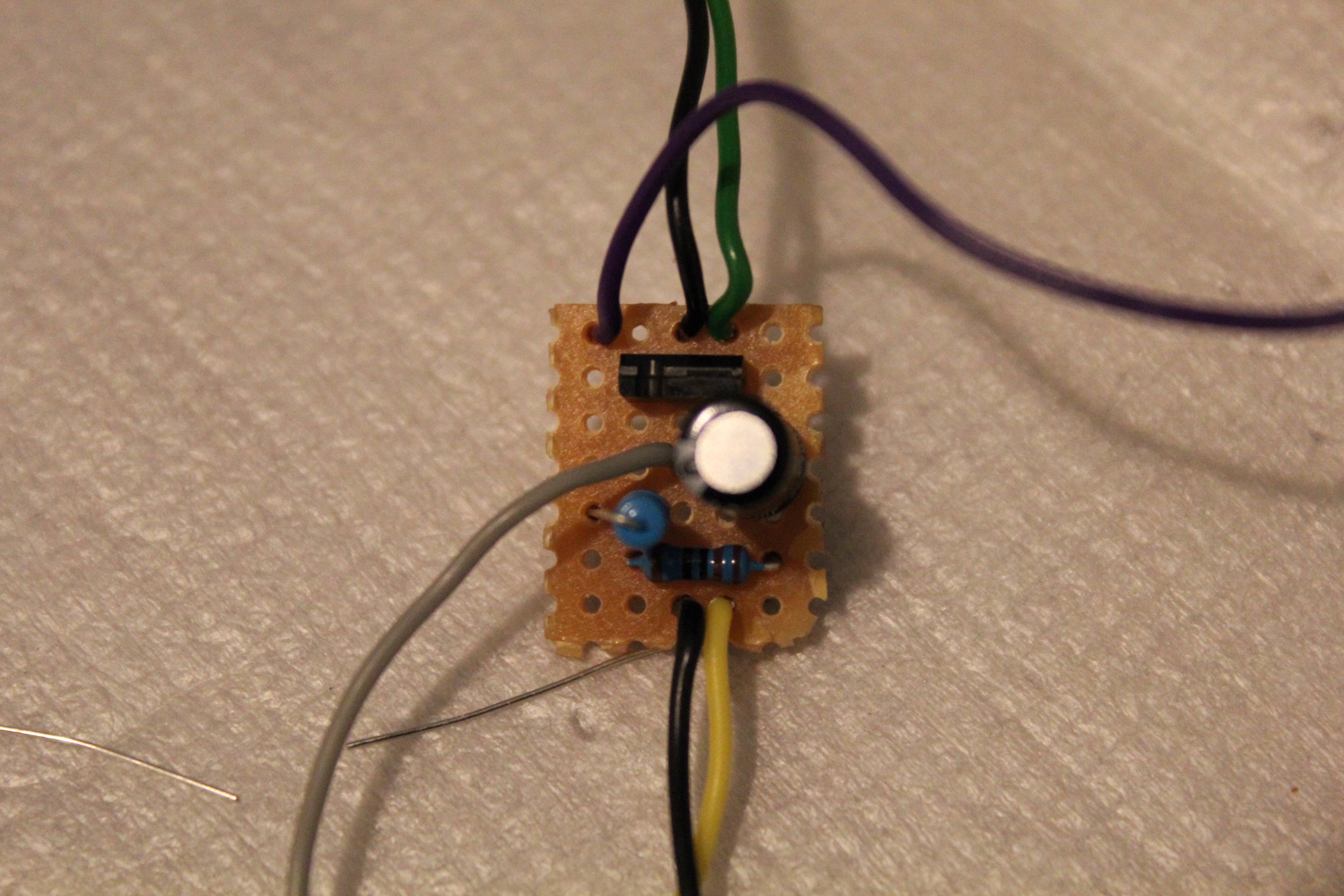
The final version was shrunk down to fit on a smaller piece of prototyping board. A much better piece of hardware.
Parts Required
– 1x 110 ohm resistor (I used 110 ohm, 0.25 watt 1% tolerance, no voltage specified).
– 1x 300 ohm resistor (I used 300 ohm, 0.5 watt 5% tolerance, 350V).
– 2x 16V 220uF 105°C electrolytic capacitor.
– 1x PNP transistor (You can remove this from the Famicom mainboard).
– Flexible light duty hook up wire or even better, kynar (I used 10 x 0.12mm cable).
– 7 x 5 hole prototyping board / veroboard.
– 25W / 40W soldering iron and solder.
– RCA Cables, plugs and sockets / jacks.
To make it all come together and actually give us AV composite you are going to need to do the following. Read on!
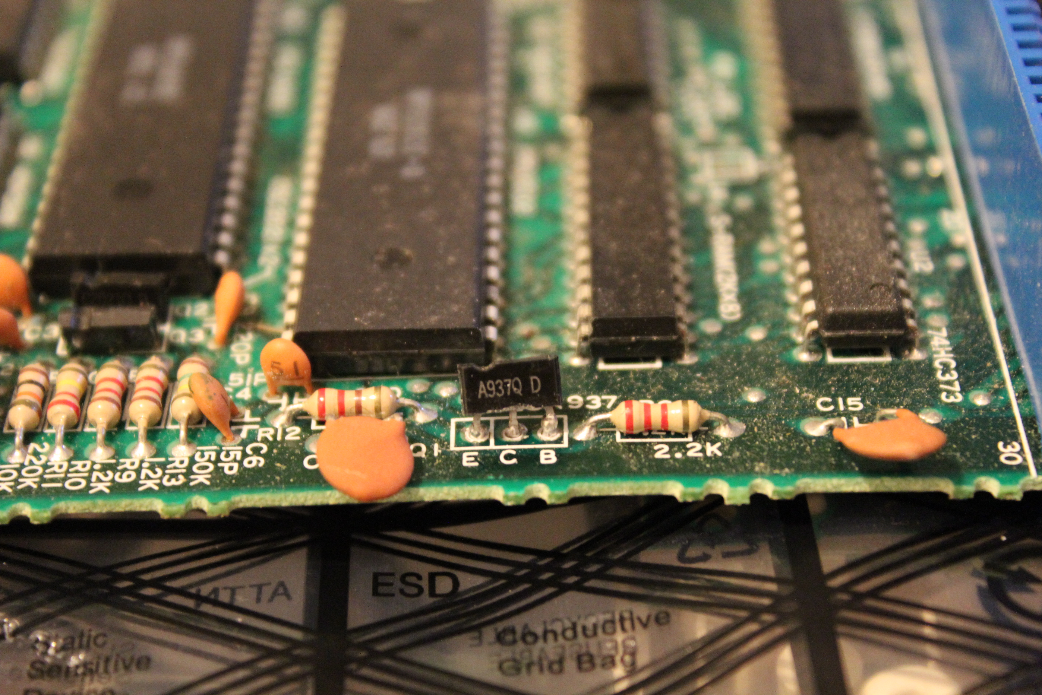
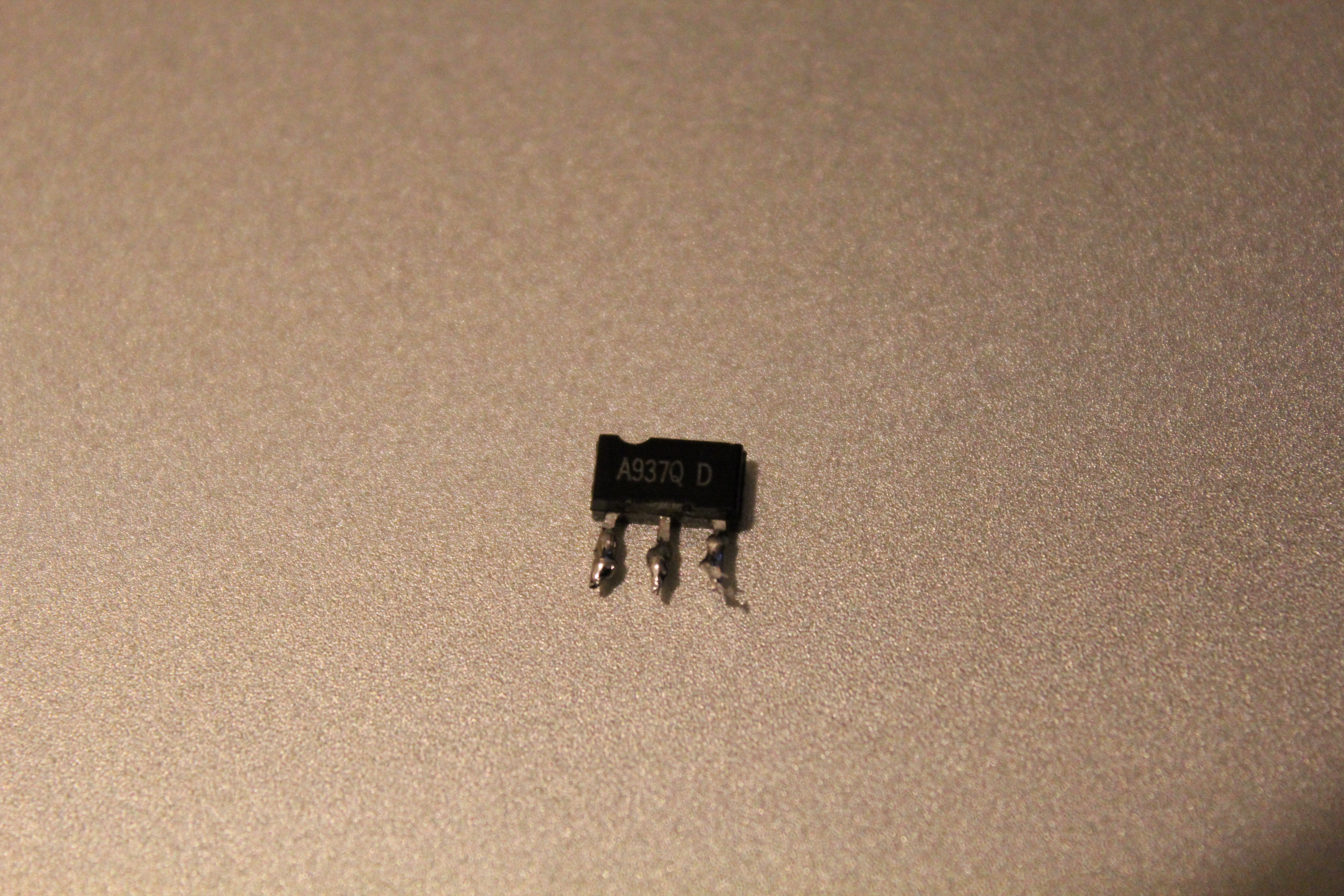

Firstly, desolder the PNP transistor (three pin component – see above) from the mainboard. If you wedge a flatblade screwdriver underneath the transistor it will greatly help with removing it. Try and heat the three legs as fast and evenly as possible. It will take some time but keep at it and you’ll get there. Be careful not to overheat the component, while they are pretty solid and can take a fair amount of heat – the less the better though! If you have desolder braid or a desolder pump you might be better off.


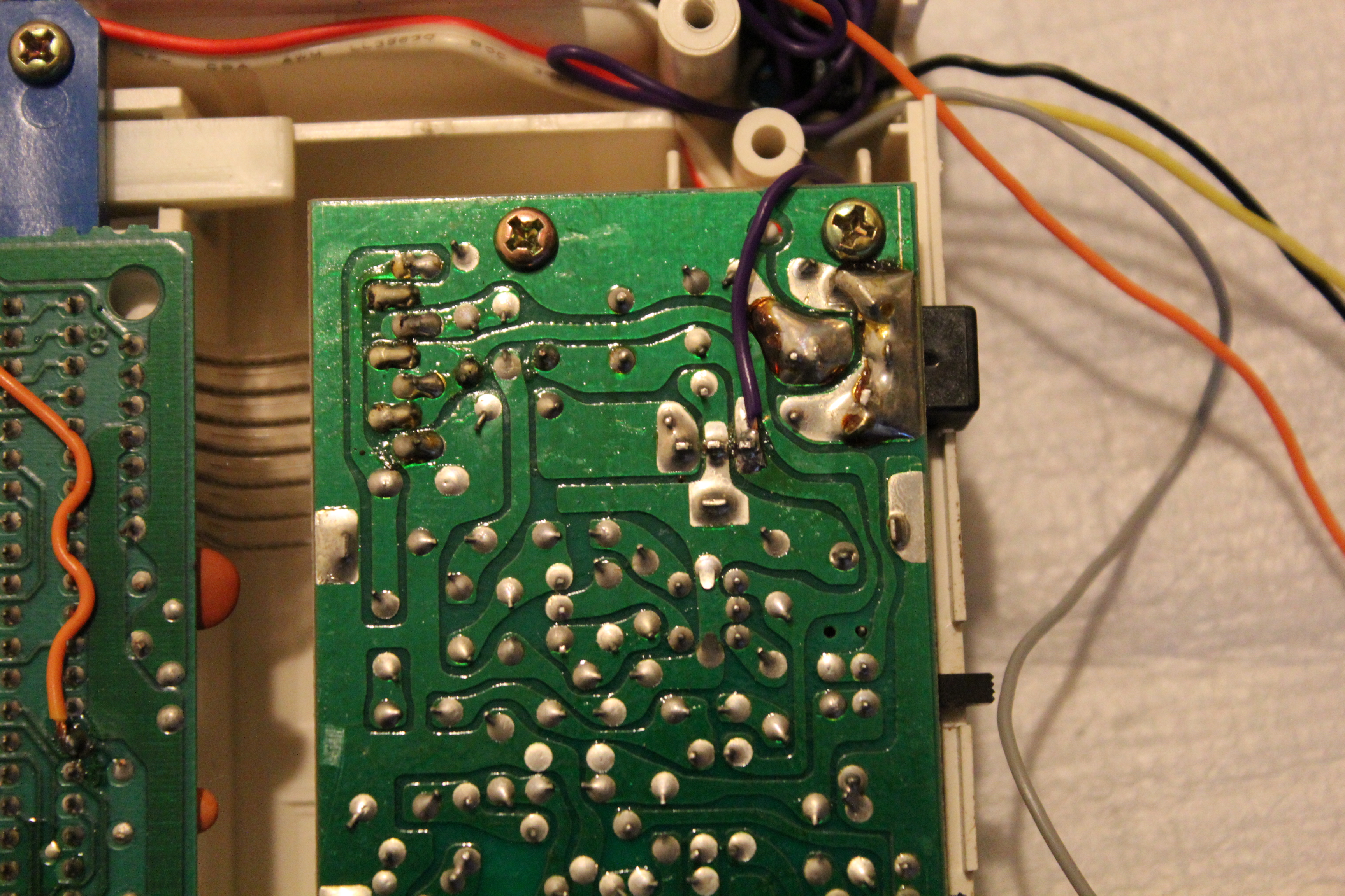
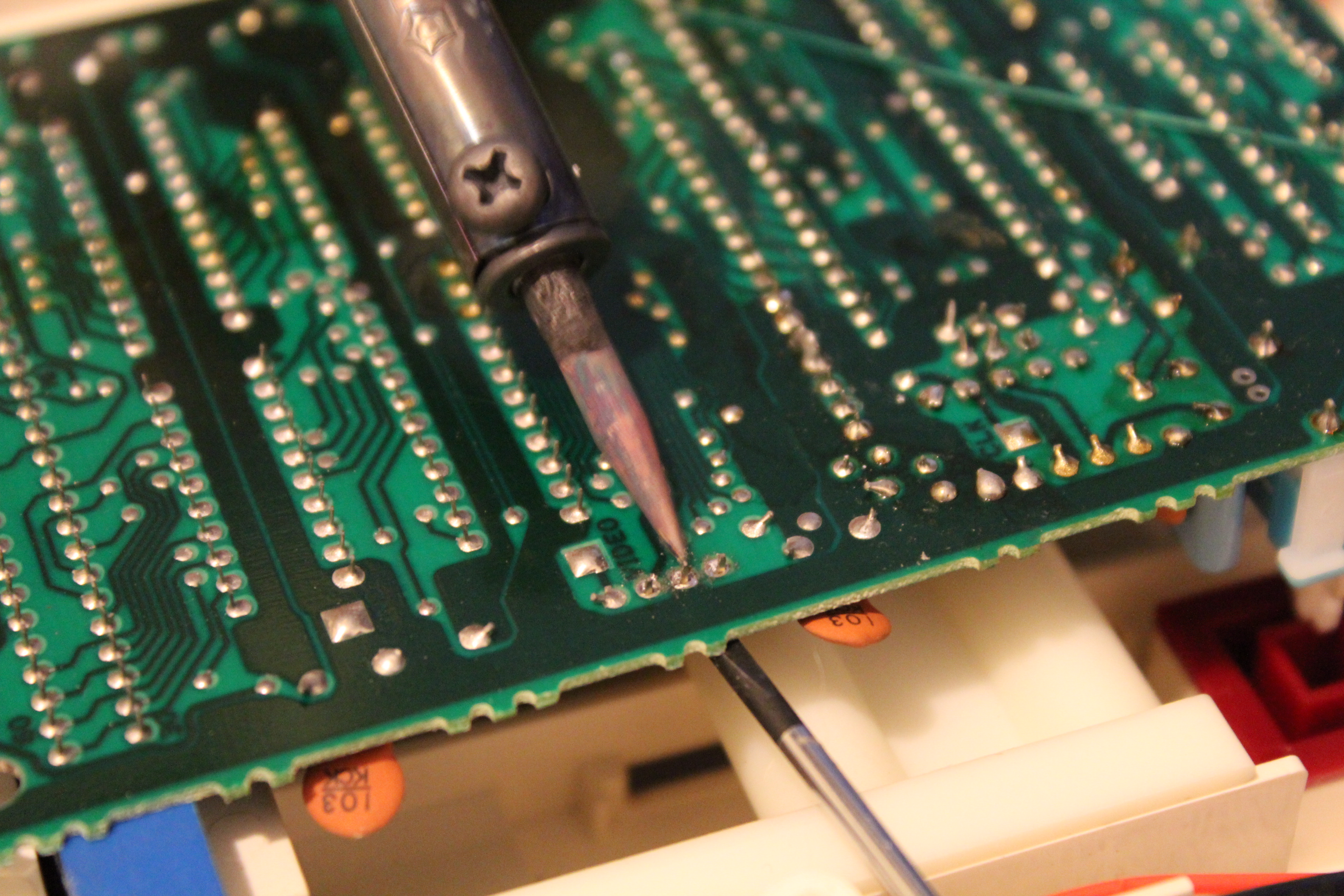
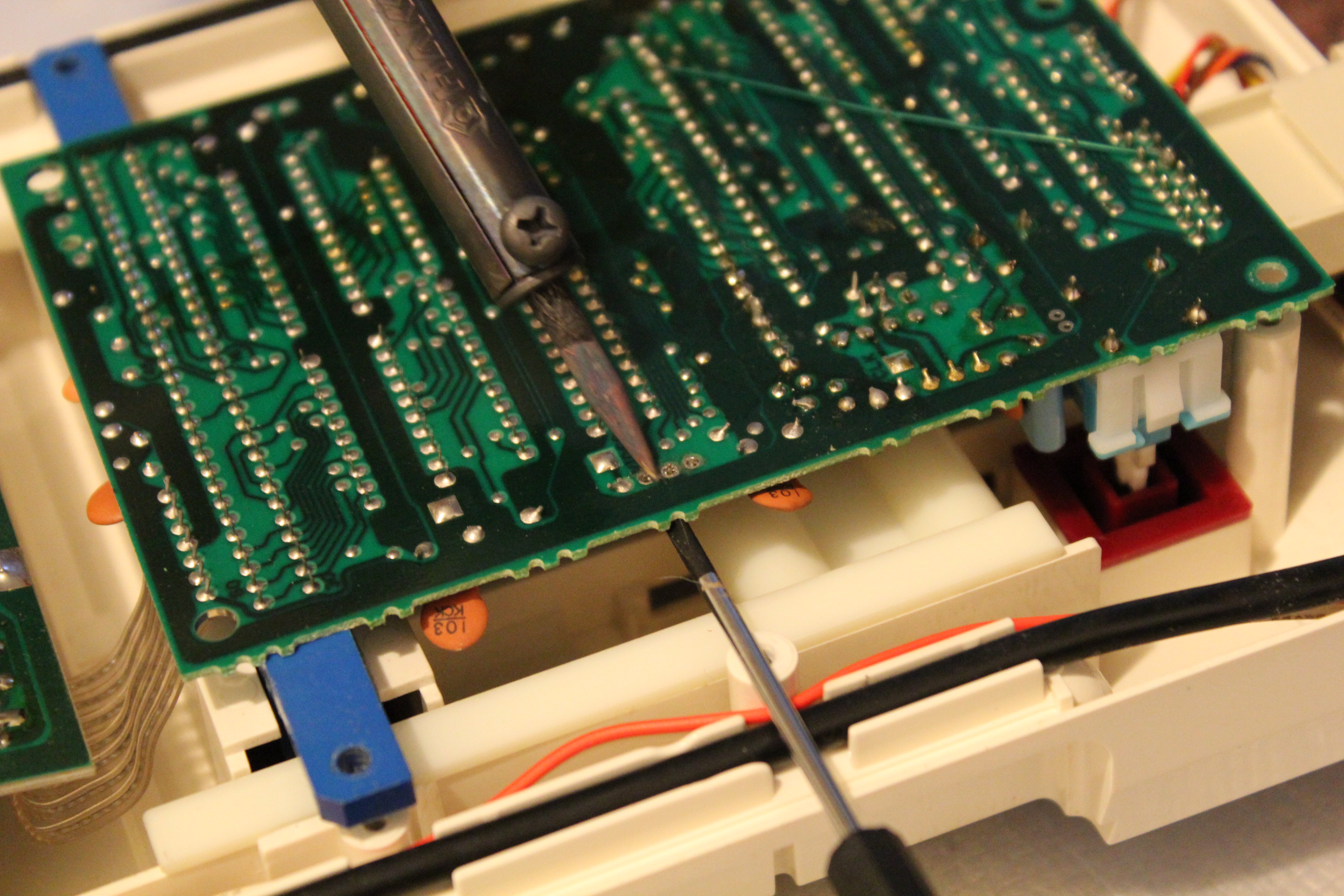
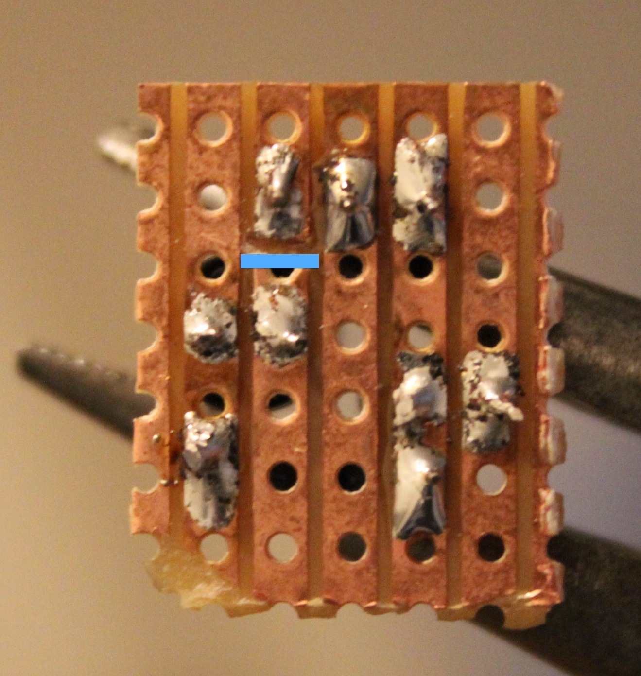
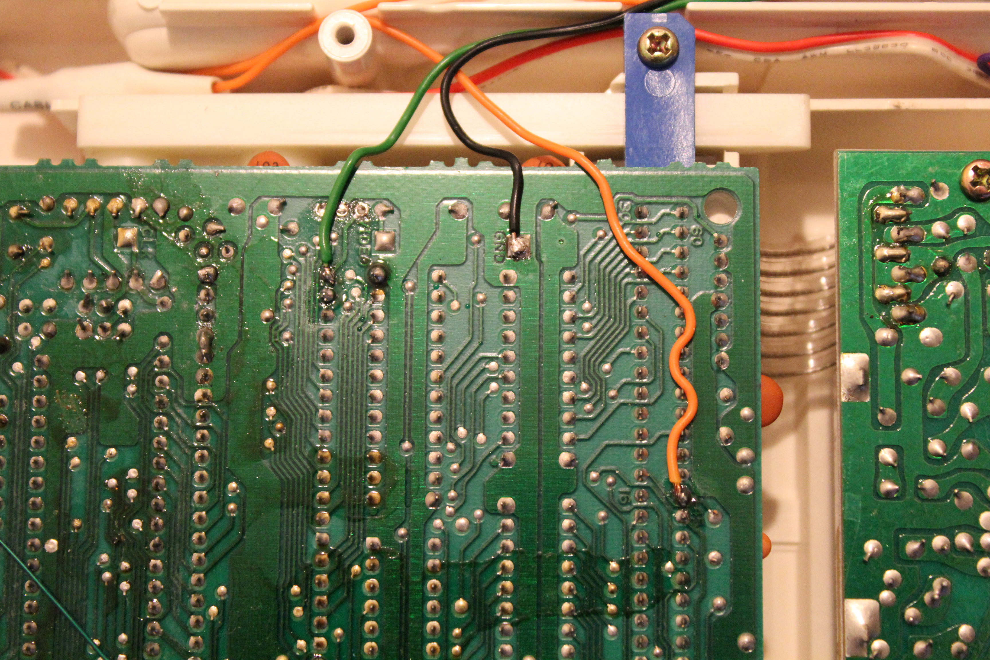
Next identify the four solder points required from the above photos. If your mainboard looks different, you have a model that is not this one. Sadly, I cannot help you with that.
The top cable (purple) taps into the voltage regulator (LM7805) and provides us with a +5V power source.

The next cable (orange) is where we get our sound source from. You’ll realise that you need two cables for sound, the other being ground – that’s the next cable we’ll look at.
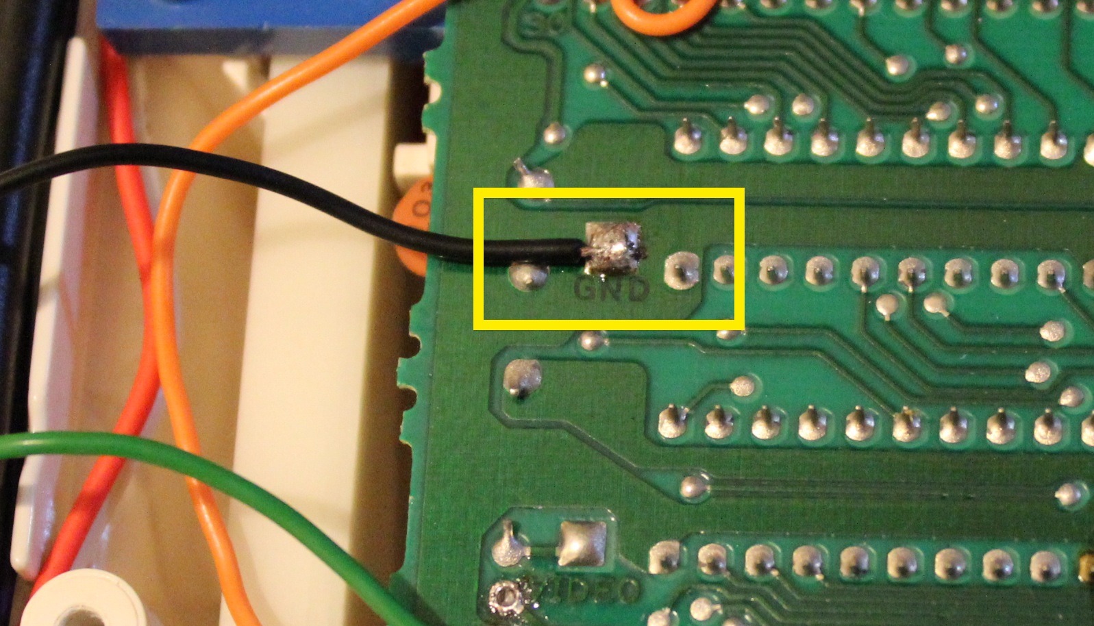
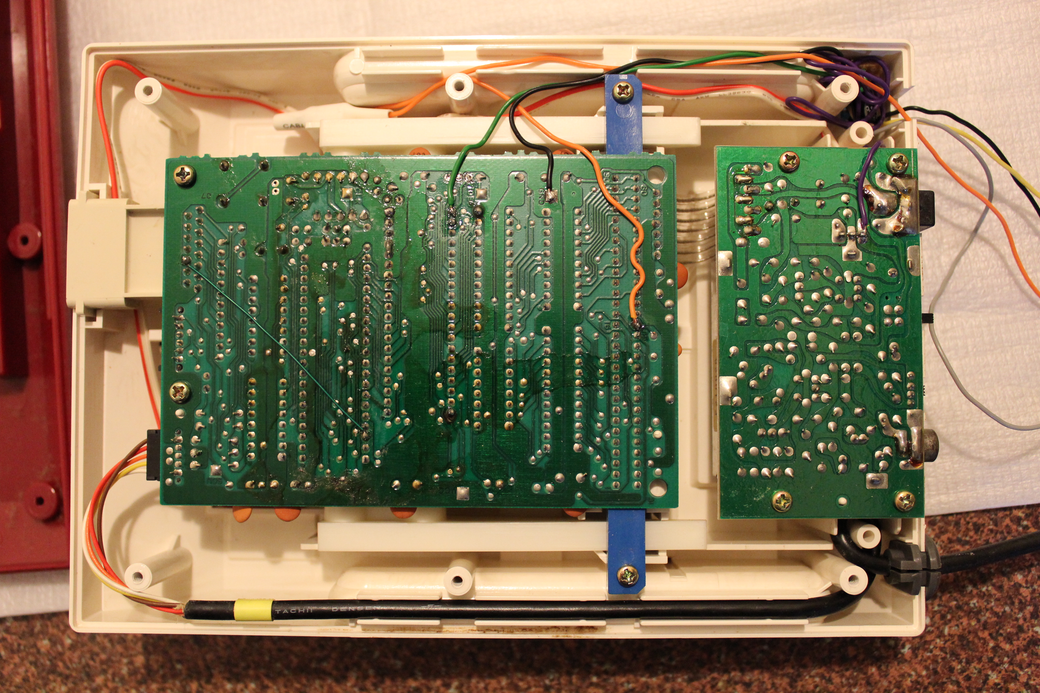
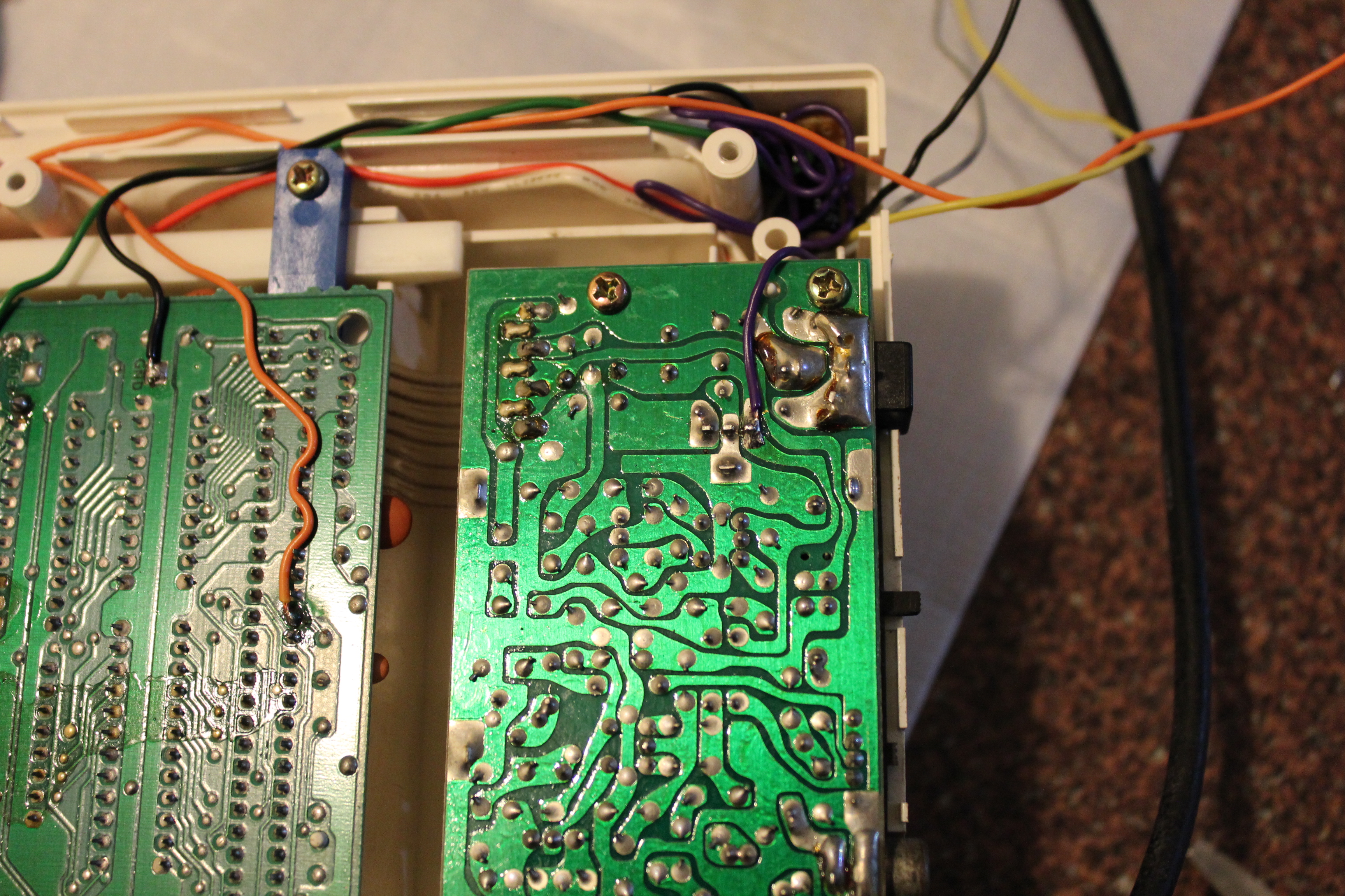
The ground point cable (black) is where you wire all your grounds into. If you see a ground, it needs to make contact with this point. I ran a cable away from it to the prototyping board and split it off into three cables from there. We’ll get to that later.
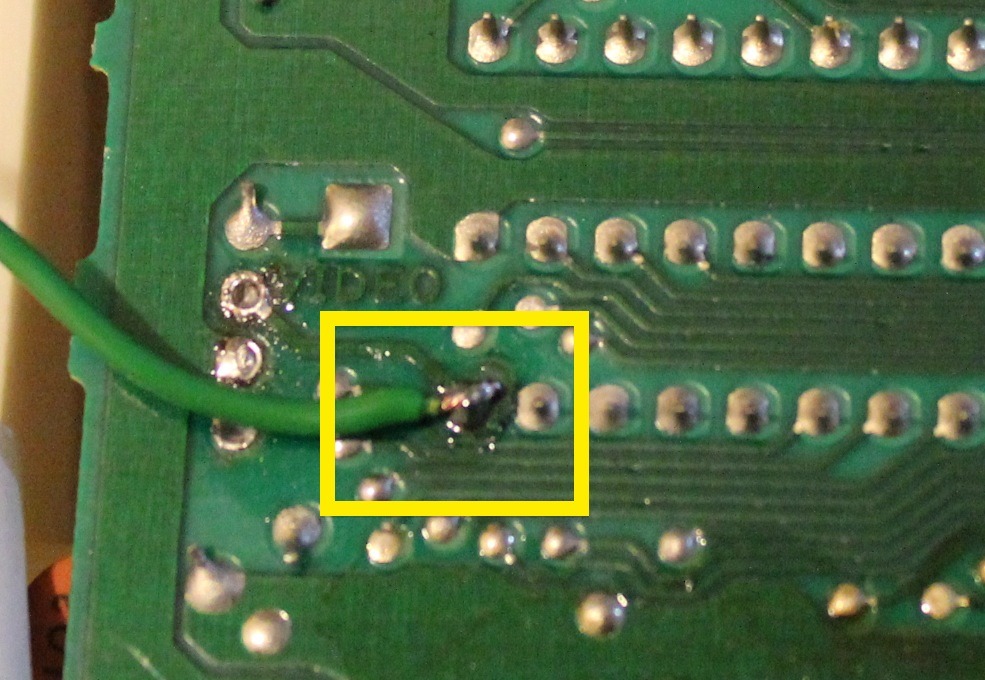
The final point is the video signal cable (green). Like the sound the AV cable will require two cables, one is the source (this!) and the other goes to ground – just like the sound will. Think of it as if the video point on the mainboard is the positive terminal and it needs to connect into a negative terminal (ground) to work properly.
The best method for soldering to these points is to reflow the solder. This way the solder will be nice and fresh and have great conductivity with the new cables you are adding. To do this you pretty much apply heat to the joint melting the existing solder and add some fresh solder in. I usually add enough so I do not have to tin the cables I am installing (Yes… I know… It sure is lazy isn’t it!).
Once you have added in your four cables, grab your prototyping board. It is time to use a knife, flatblade or hacksaw (I used this once…) to cut the board down to size.
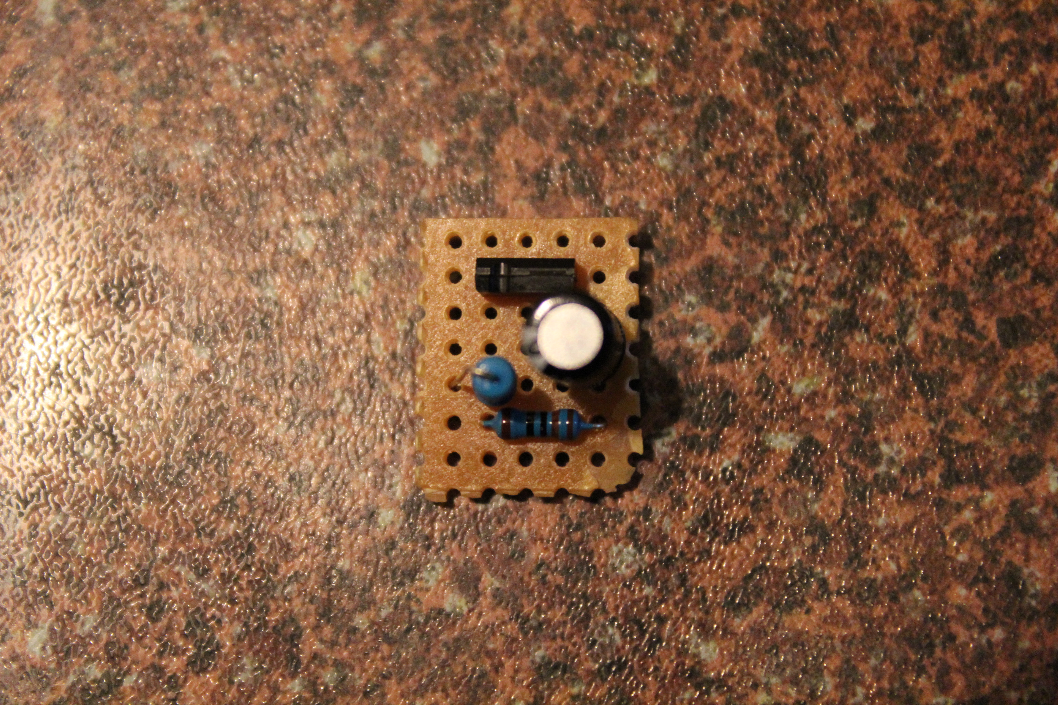

As you can see above the board size I used has 5 x 7 holes. It also gives you an idea of the layout. Install all the components as you can see them in the pictures. Resistors do not mind polarity. Be very careful to ensure you get the capacitor installed the correct way around – they are polar!
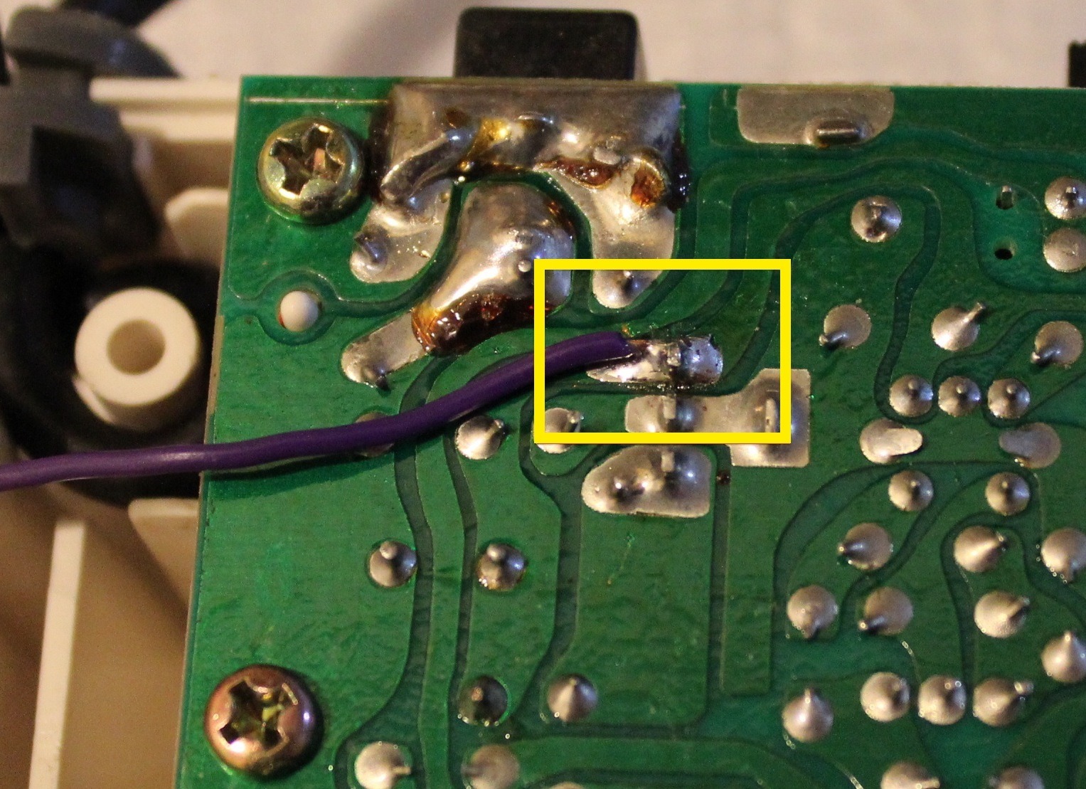
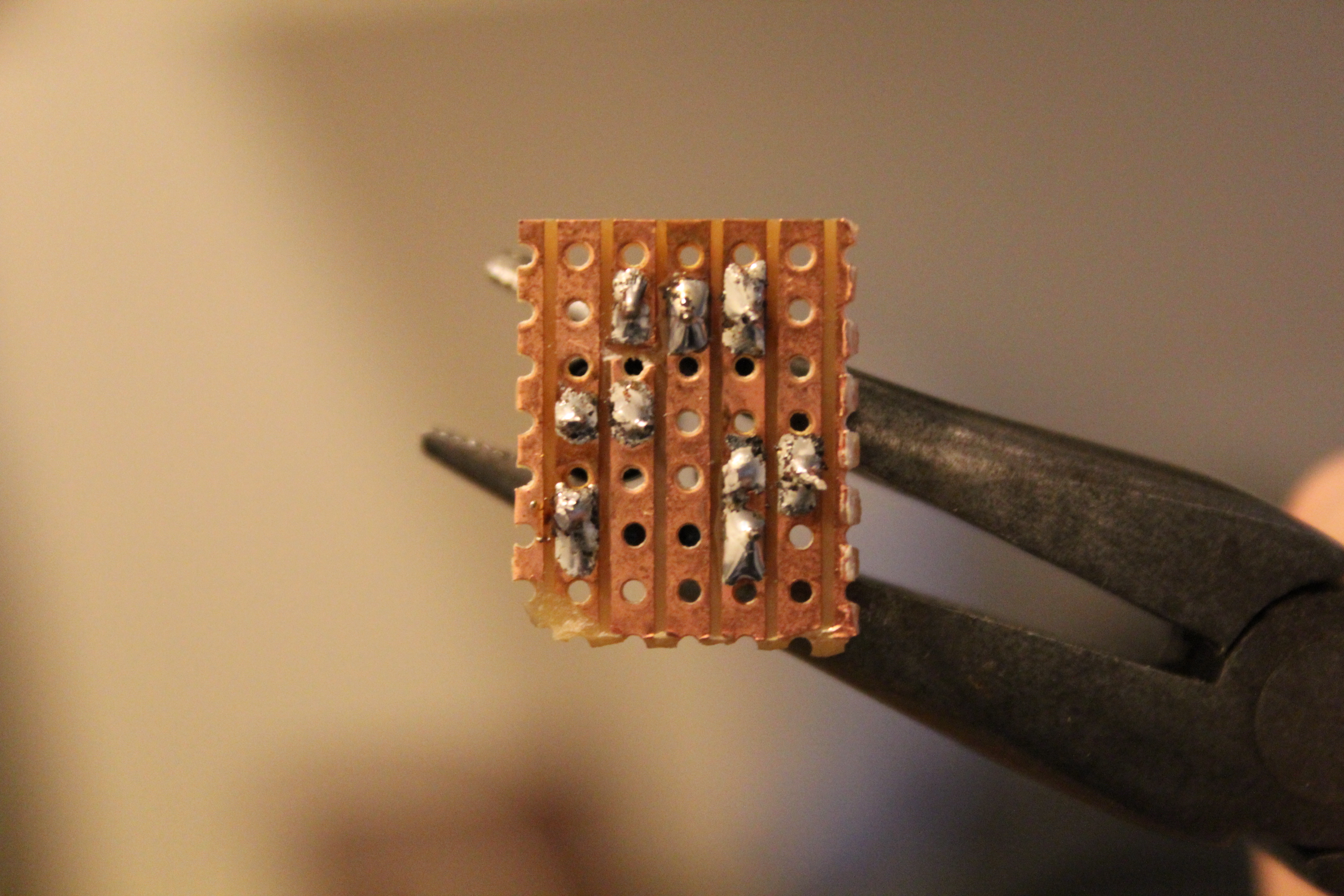
The track in the photo above has been cut on the underside of the board to prevent the capacitor juicing up the wrong components. Make sure that this one track is cut. I used a flatblade screwdriver to scrape away at the copper track. Use a multimeter to ensure there is no continuity between the two ends of the board once it has been scraped away. Failing to do this may result in a bit of a bang and some flames to boot.
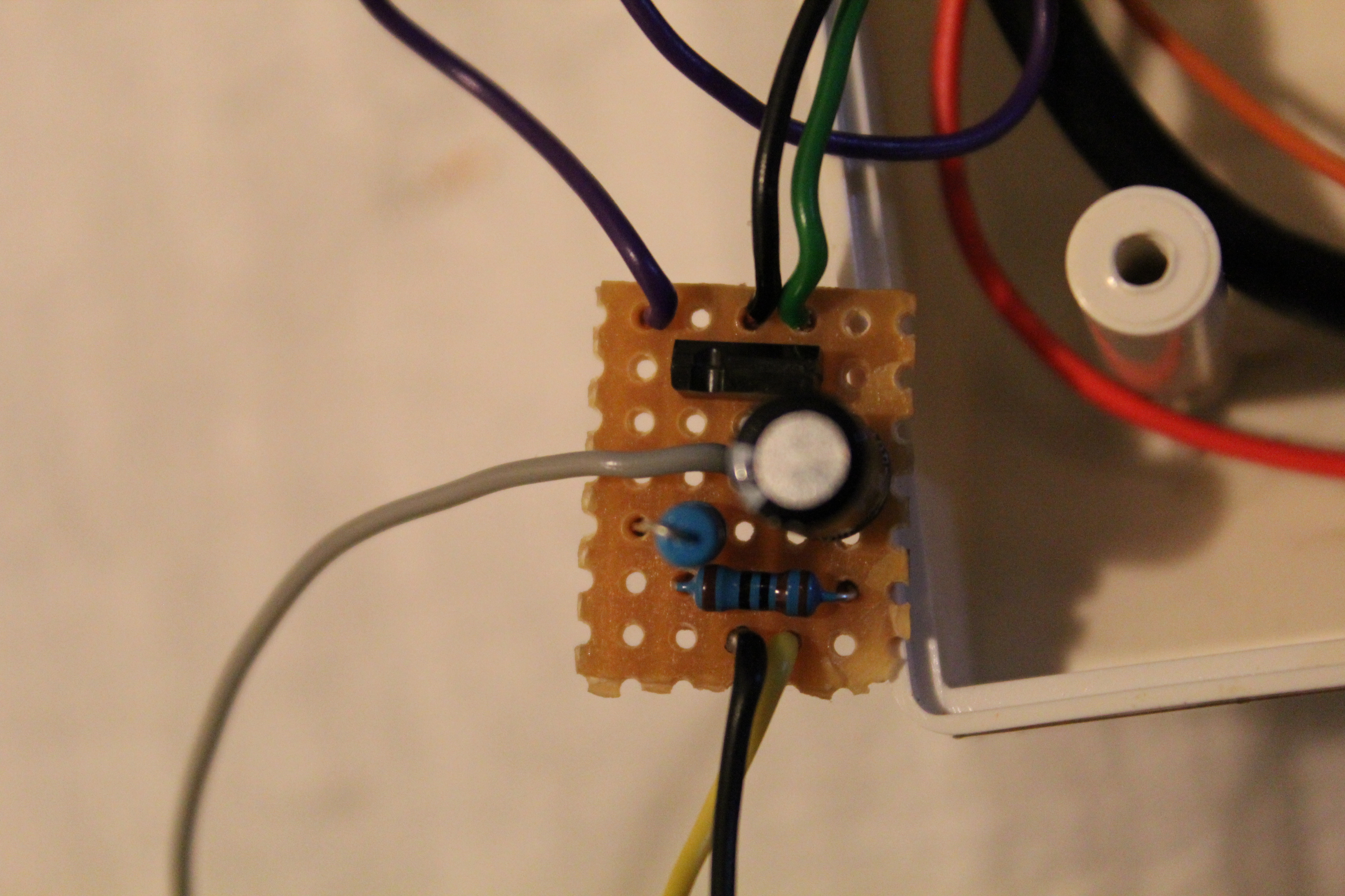

What are all those coloured cables above? Purple is the +5V coming in from the voltage regulator (LM7805). Green is the video signal entering from the mainboard. The blacks and the grey (ran out of black) are all ground. One runs to the mainboard. The other two are for sound and video (although one ground cable can be used for both if you really want to). Yellow is video out that goes to the centre plug of the TV RCA jack.

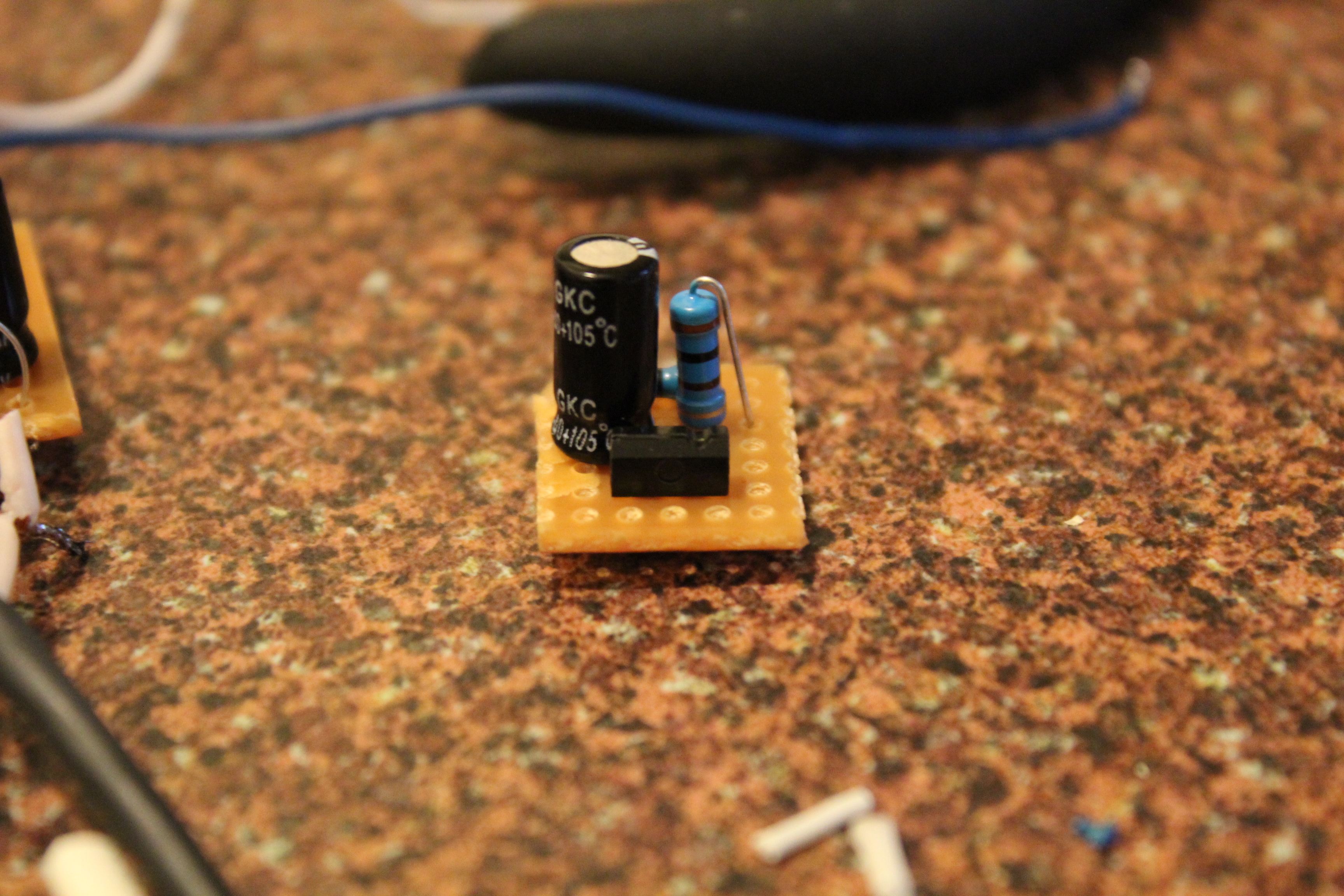
Be sure to solder the transistor you desoldered from the Famicom on the right way with the notch facing the correct side. Otherwise things will go funky and possibly explode. Once all this is done you should be able to get video to show on your TV screen. If nothing shows or you see flames, disconnect the unit from mains power and check your soldering and polarities.
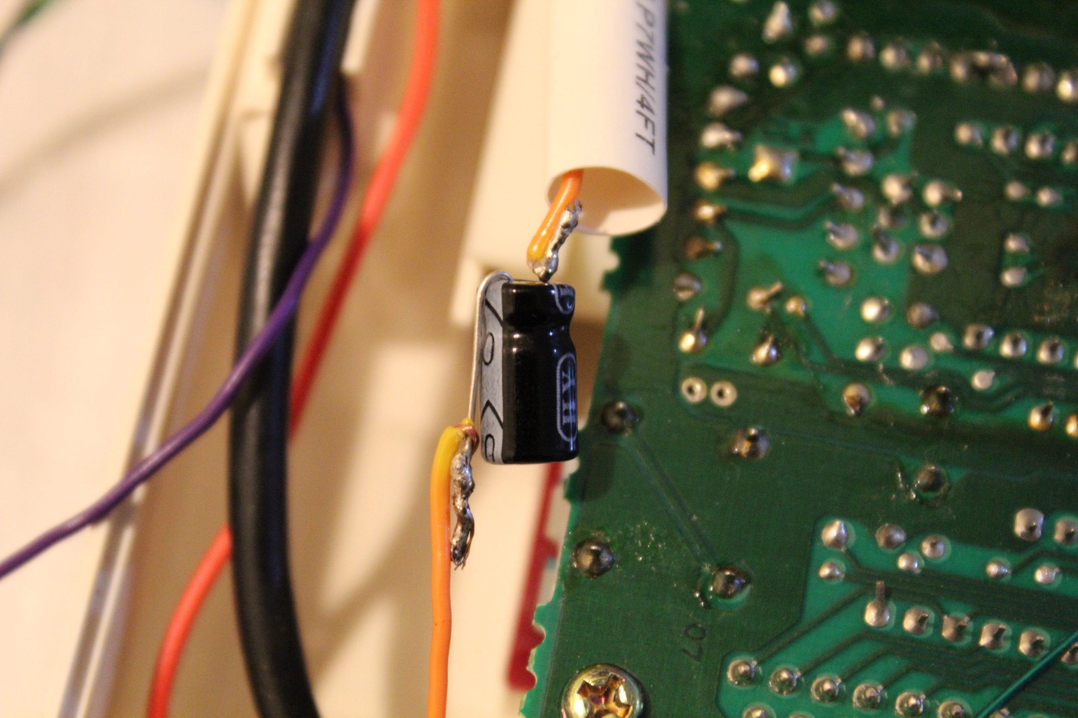
Next we move onto the sound, which is relatively easy. That orange cable that runs from pin 46 on the mainboard in the photos above needs to run into a 16V 220uF capacitor. Positive end goes toward the mainboard end as you are feeding the capacitor with voltage and then negative runs out of it. This other end then leads to your sound RCA cable (centre pin). Couple it with a ground cable and you are done. Make sure you get that polarity the right way around.
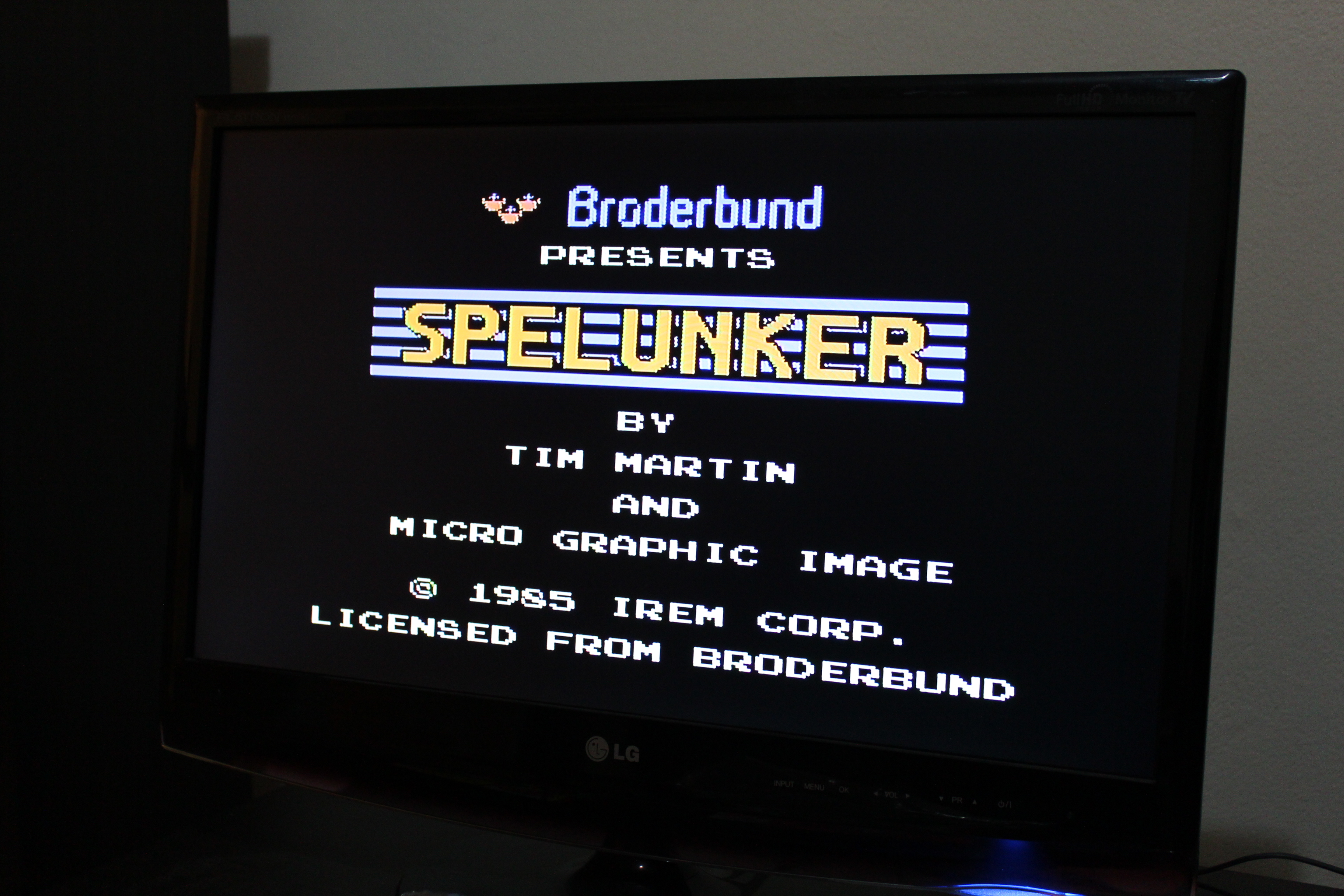
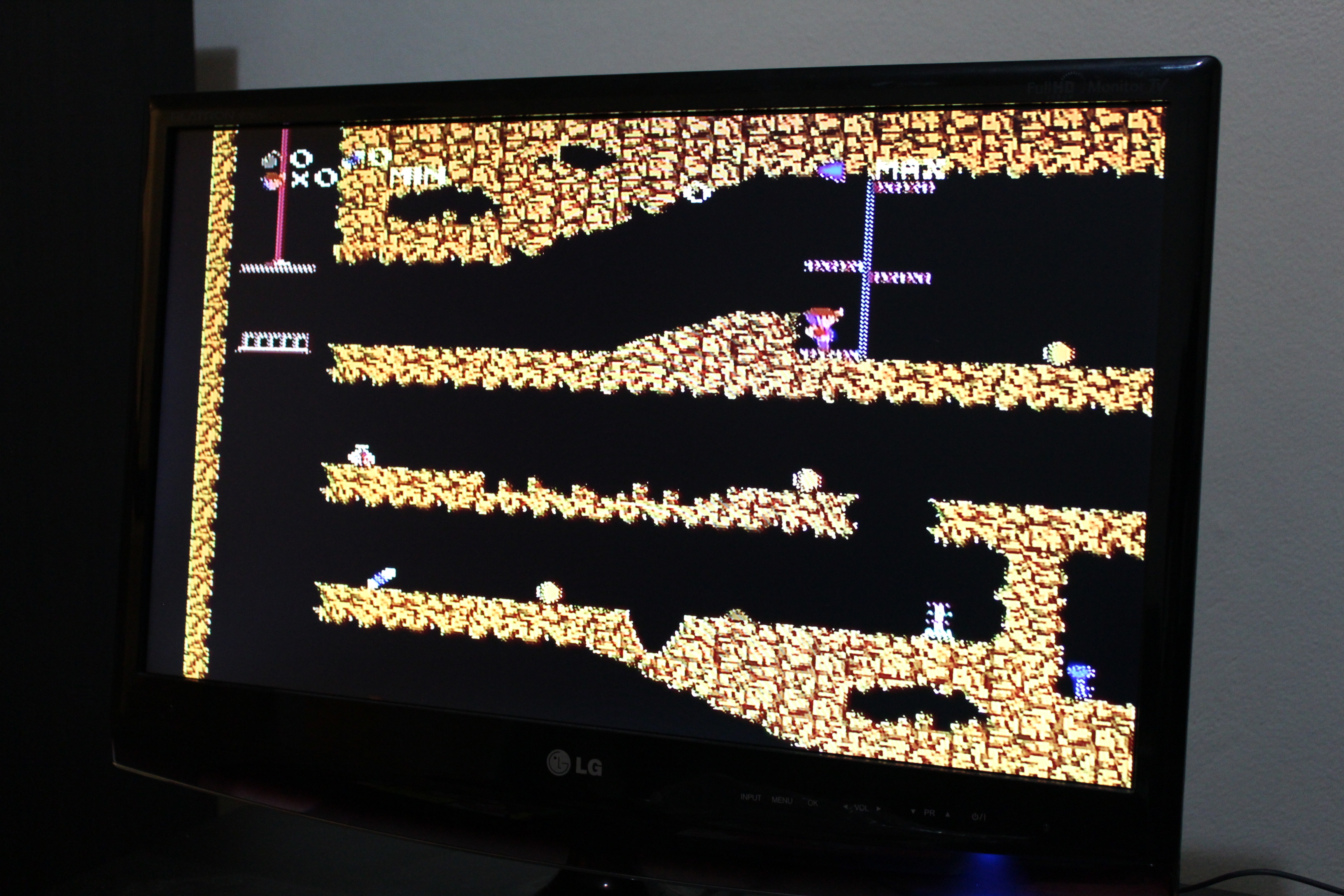
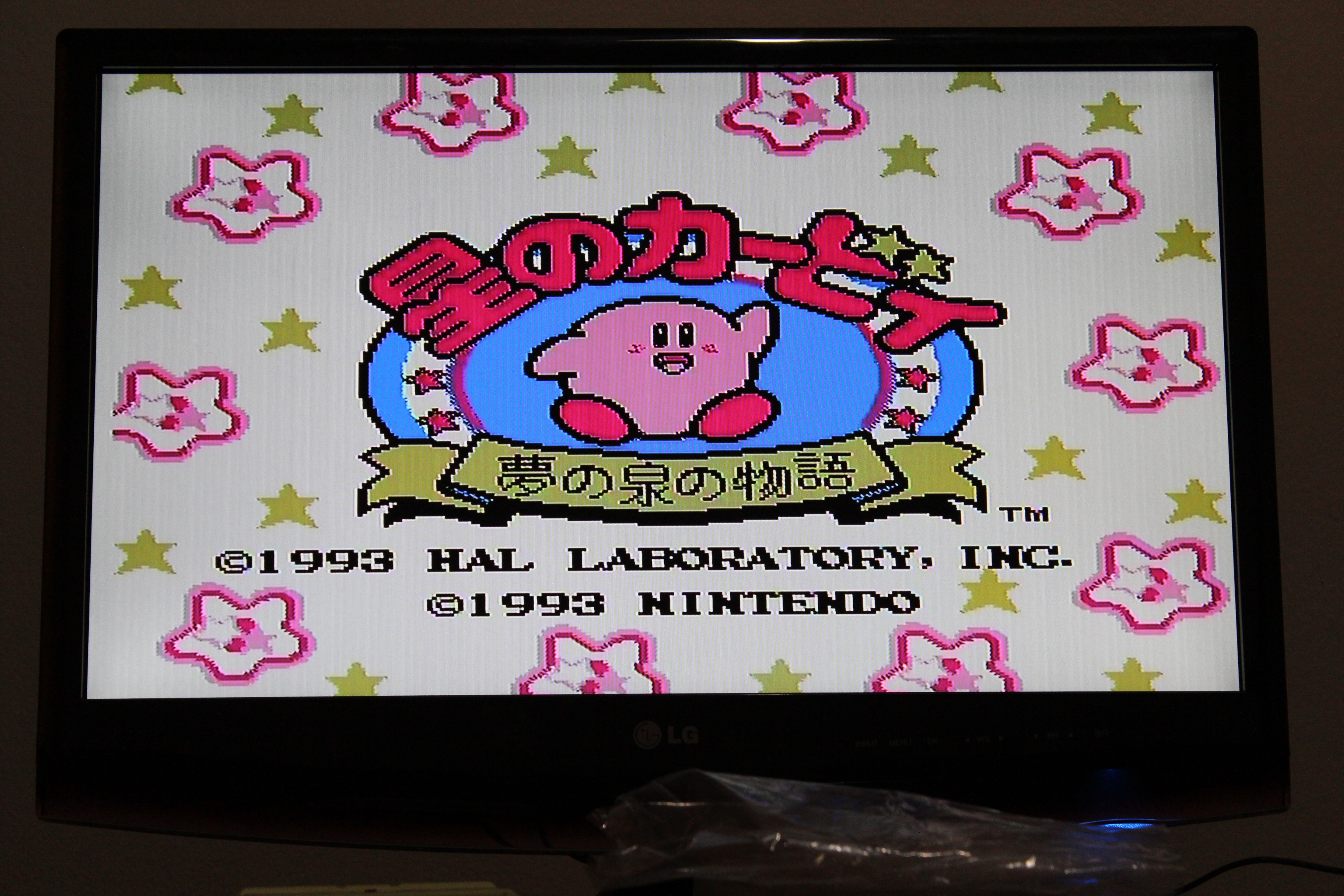
Now all that’s left is to enjoy your Kirby and Spelunker! Below are some videos of the unit while it was in pieces explaining where cables run and what their ratings are.
Additionally you can try to remove the jail bars that show by checking out this link here. This was the original guide that I followed. It has good schematics too if you are a schematicky sort of person. I had no luck with any of the jail bar reducing / removing methods listed. Your luck may vary. Good luck!
Resources: Another Nintendo Famicom AV Mod
McRetro Photo Gallery